General Description
The DS3231 is a low-cost, extremely accurate I2C real-time clock (RTC) with an integrated temperature-compensated crystal oscillator (TCXO) and crystal. The device incorporates a battery input, and maintains accu-rate timekeeping when main power to the device is inter-rupted. The integration of the crystal resonator enhances the long-term accuracy of the device as well as reduces the piece-part count in a manufacturing line. The DS3231 is available in commercial and industrial temperature ranges, and is offered in a 16-pin, 300-mil SO package. The RTC maintains seconds, minutes, hours, day, date, month, and year information. The date at the end of the month is automatically adjusted for months with fewer than 31 days, including corrections for leap year. The clock operates in either the 24-hour or 12-hour format with an AM/PM indicator. Two programmable time-of-day alarms and a programmable square-wave output are provided. Address and data are transferred serially through an I2C bidirectional bus.A precision temperature-compensated voltage refer-ence and comparator circuit monitors the status of VCC to detect power failures, to provide a reset output, and to automatically switch to the backup supply when nec-essary. Additionally, the RST pin is monitored as a pushbutton input for generating a reset externally.
Applications
Servers Utility Power Meters
Telematics GPS
Features
♦ Accuracy ±2ppm from 0°C to +40°C
♦ Accuracy ±3.5ppm from -40°C to +85°C
♦ Battery Backup Input for Continuous
Timekeeping
♦ Operating Temperature Ranges
Commercial: 0°C to +70°C Industrial: -40°C to +85°C
♦ Low-Power Consumption
♦ Real-Time Clock Counts Seconds, Minutes,
Hours, Day, Date, Month, and Year with Leap Year Compensation Valid Up to 2100
♦ Two Time-of-Day Alarms
♦ Programmable Square-Wave Output
♦ Fast (400kHz) I2C Interface
♦ 3.3V Operation
♦ Digital Temp Sensor Output: ±3°C Accuracy
♦ Register for Aging Trim
♦ RSTInput/Output
♦ UL Recognized
DS3231
RTC/TCXO/Crystal
Ordering Information
PART TEMP RANGE PIN-PACKAGE TOP
MARK
DS3231S 0°C to +70°C 16 SO DS3231
DS3231SN -40°C to +85°C 16 SO DS3231N
DS3231S+ 0°C to +70°C 16 SO DS3231+
DS3231SN+ -40°C to +85°C 16 SO DS3231N+
Pin Configuration appears at end of data sheet.
VCC
SCL RPU
RPU = tR/CB
RPU
INT/SQW
32kHz SDA
VCC
VCC
VCC
CPU
Typical Operating Circuit
DS3231
ABSOLUTE MAXIMUM RATINGS
RECOMMENDED DC OPERATING CONDITIONS
(TA= TMINto TMAX, unless otherwise noted.) (Notes 1, 2)Stresses beyond those listed under “Absolute Maximum Ratings” may cause permanent damage to the device. These are stress ratings only, and functional operation of the device at these or any other conditions beyond those indicated in the operational sections of the specifications is not implied. Exposure to absolute maximum rating conditions for extended periods may affect device reliability.
Voltage Range on VCC, VBAT, 32kHz, SCL, SDA, RST,
INT/SQW Relative to Ground...-0.3V to +6.0V Operating Temperature Range
(noncondensing) ...-40°C to +85°C Junction Temperature ...+125°C
Storage Temperature Range ...-40°C to +85°C Lead Temperature
(Soldering, 10s)...+260°C/10s Soldering Temperature...See the Handling,
PC Board Layout, and Assemblysection.
PARAMETER SYMBOL CONDITIONS MIN TYP MAX UNITS
VCC 2.3 3.3 5.5 V
Supply Voltage
VBAT 2.3 3.0 5.5 V
Logic 1 Input SDA, SCL VIH 0.7 x
VCC
VCC +
0.3 V
Logic 0 Input SDA, SCL VIL -0.3 +0.3 x
VCC V
Pullup Voltage
(SDA, SCL, 32kHz, INT/SQW) VPU VCC = 0V 5.5V V
ELECTRICAL CHARACTERISTICS
(VCC= 2.3V to 5.5V, VCC> VBAT, TA= TMINto TMAX, unless otherwise noted.) (Typical values are at VCC = 3.3V, VBAT= 3.0V, and TA= +25°C, unless otherwise noted.) (Notes 1, 2)
PARAMETER SYMBOL CONDITIONS MIN TYP MAX UNITS
VCC = 3.63V 200
Active Supply Current ICCA (Notes 3, 4)
VCC = 5.5V 300
µA
VCC = 3.63V 110
Standby Supply Current ICCS
I2C bus inactive, 32kHz output on, SQW output off
(Note 4) VCC = 5.5V 170
µA
VCC = 3.63V 575
Temperature Conversion Current ICCSCONV I
2C bus inactive, 32kHz
output on, SQW output off VCC = 5.5V 650
µA
Power-Fail Voltage VPF 2.45 2.575 2.70 V
Logic 0 Output, 32kHz, INT/SQW,
SDA VOL IOL = 3mA 0.4 V
Logic 0 Output, RST VOL IOL = 1mA 0.4 V
Output Leakage Current 32kHz,
INT/SQW, SDA ILO Output high impedance -1 0 +1 µA
Input Leakage SCL ILI -1 +1 µA
RST Pin I/O Leakage IOL RST high impedance (Note 5) -200 +10 µA
VBAT Leakage Current
DS3231
ELECTRICAL CHARACTERISTICS (continued)
(VCC= 2.3V to 5.5V, VCC> VBAT, TA= TMINto TMAX, unless otherwise noted.) (Typical values are at VCC = 3.3V, VBAT= 3.0V, and TA= +25°C, unless otherwise noted.) (Notes 1, 2)
PARAMETER SYMBOL CONDITIONS MIN TYP MAX UNITS
Output Frequency fOUT VCC = 3.3V or VBAT = 3.3V 32.768 kHz
0°C to +40°C ±2
Frequency Stability vs.
Temperature (Commercial) ∆f/fOUT
VCC = 3.3V or VBAT = 3.3V,
aging offset = 00h >40°C to +70°C ±3.5
ppm
-40°C to <0°C ±3.5
0°C to +40°C ±2
Frequency Stability vs.
Temperature (Industrial) ∆f/fOUT
VCC = 3.3V or VBAT = 3.3V,
aging offset = 00h >40°C to +85°C ±3.5
ppm
Frequency Stability vs. Voltage ∆f/V 1 ppm/V
-40°C 0.7
+25°C 0.1
+70°C 0.4
Trim Register Frequency
Sensitivity per LSB ∆f/LSB Specified at:
+85°C 0.8
ppm
Temperature Accuracy Temp VCC = 3.3V or VBAT = 3.3V -3 +3 °C
First year ±1.0
Crystal Aging ∆f/f0 After reflow,
not production tested 0–10 years ±5.0 ppm
ELECTRICAL CHARACTERISTICS
(VCC= 0V, VBAT= 2.3V to 5.5V, TA= TMINto TMAX, unless otherw.ise noted.) (Note 1)
PARAMETER SYMBOL CONDITIONS MIN TYP MAX UNITS
VBAT = 3.63V 70
Active Battery Current IBATA
EOSC = 0, BBSQW = 0,
SCL = 400kHz (Note 4) VBAT = 5.5V 150
µA
VBAT = 3.63V 0.84 3.0
Timekeeping Battery Current IBATT
EOSC = 0, BBSQW = 0, EN32kHz = 1,
SCL = SDA = 0V or
S C L = S D A = VBAT ( Note 4) VBAT = 5.5V 1.0 3.5
µA
VBAT = 3.63V 575
Temperature Conversion Current I
EOSC = 0, BBSQW = 0,
DS3231
AC ELECTRICAL CHARACTERISTICS
(VCC= VCC(MIN)to VCC(MAX)or VBAT= VBAT(MIN)to VBAT(MAX), VBAT> VCC, TA= TMINto TMAX, unless otherwise noted.) (Note 1)
PARAMETER SYMBOL CONDITIONS MIN TYP MAX UNITS
Fast mode 100 400
SCL Clock Frequency fSCL
Standard mode 0 100 kHz
Fast mode 1.3
Bus Free Time Between STOP
and START Conditions tBUF Standard mode 4.7 µs
Fast mode 0.6
Hold Time (Repeated) START
Condition (Note 6) tHD:STA Standard mode 4.0 µs
Fast mode 1.3
Low Period of SCL Clock tLOW
Standard mode 4.7 µs
Fast mode 0.6
High Period of SCL Clock tHIGH
Standard mode 4.0 µs
Fast mode 0 0.9
Data Hold Time (Notes 7, 8) tHD:DAT
Standard mode 0 0.9 µs
Fast mode 100
Data Setup Time (Note 9) tSU:DAT
Standard mode 250 ns
Fast mode 0.6
Start Setup Time tSU:STA
Standard mode 4.7 µs
Fast mode 300
Rise Time of Both SDA and SCL
Signals (Note 10) tR Standard mode
20 +
0.1CB 1000 ns
Fast mode 300
Fall Time of Both SDA and SCL
Signals (Note 10) tF Standard mode
20 +
0.1CB 300 ns
Fast mode 0.6
Setup Time for STOP Condition tSU:STO
Standard mode 4.7 µs
Capacitive Load for Each Bus
Line (Note 10) CB 400 pF
Capacitance for SDA, SCL CI/O 10 pF
Pulse Width of Spikes That Must
Be Suppressed by the Input Filter tSP 30 ns
Pushbutton Debounce PBDB 250 ms
Reset Active Time tRST 250 ms
Oscillator Stop Flag (OSF) Delay tOSF (Note 11) 100 ms
Temperature Conversion Time tCONV 125 200 ms
POWER-SWITCH CHARACTERISTICS
(TA= TMINto TMAX)PARAMETER SYMBOL CONDITIONS MIN TYP MAX UNITS
VCC Fall Time; VPF(MAX) to
VPF(MIN) tVCCF 300 µs
VCC Rise Time; VPF(MIN) to
VPF(MAX) tVCCR 0 µs
DS3231
Pushbutton Reset Timing
tRST
PBDB
RST
Power-Switch Timing
VCC
tVCCF tVCCR
tREC
VPF(MAX)
VPF VPF
VPF(MIN)
DS3231
Data Transfer on I
2
C Serial Bus
SDA
SCL
tHD:STA
tLOW
tHIGH
tR tF
tBUF
tHD:DAT
tSU:DAT REPEATED
START tSU:STA
tHD:STA
tSU:STO
tSP
STOP START
Note 1: Limits at -40°C are guaranteed by design and not production tested. Note 2: All voltages are referenced to ground.
Note 3: ICCA—SCL clocking at max frequency = 400kHz.
Note 4: Current is the averaged input current, which includes the temperature conversion current. Note 5: The RSTpin has an internal 50kΩ(nominal) pullup resistor to VCC.
Note 6: After this period, the first clock pulse is generated.
Note 7: A device must internally provide a hold time of at least 300ns for the SDA signal (referred to the VIH(MIN)of the SCL signal) to bridge the undefined region of the falling edge of SCL.
Note 8: The maximum tHD:DATneeds only to be met if the device does not stretch the low period (tLOW) of the SCL signal. Note 9: A fast-mode device can be used in a standard-mode system, but the requirement tSU:DAT≥250ns must then be met. This
is automatically the case if the device does not stretch the low period of the SCL signal. If such a device does stretch the low period of the SCL signal, it must output the next data bit to the SDA line tR(MAX)+ tSU:DAT= 1000 + 250 = 1250ns before the SCL line is released.
Note 10:CB—total capacitance of one bus line in pF.
Note 11:The parameter tOSFis the period of time the oscillator must be stopped for the OSF flag to be set over the voltage range of 0.0V ≤VCC≤VCC(MAX) and 2.3V ≤VBAT≤3.4V.
DS3231
STANDBY SUPPLY CURRENT vs. SUPPLY VOLTAGE
DS3231 toc01
VCC (V)
ICCS ( µ A) 5.0 4.0 3.0 50 100 150 0 2.0 RST ACTIVE SUPPLY CURRENT vs. SUPPLY VOLTAGE
DS3231 toc02
VBAT (V)
IBAT ( µ A) 5.0 4.0 3.0 0.800 0.900 1.000 1.100 1.200 0.700 2.0
VCC = 0V
SUPPLY CURRENT vs. TEMPERATURE
DS3231 toc03
TEMPERATURE (°C)
IBAT ( µ A) 80.0 60.0 40.0 20.0 0.0 -20.0 0.700 0.800 0.900 1.000 0.600 -40.0
VBAT = 3.0V
FREQUENCY DEVIATION vs. TEMPERATURE vs. AGING VALUE
DS3231 toc04
CRYSTAL AGING REGISTER VALUE
FREQUENCY DEVIATION (ppm)
96 64 0 32 -64 -32 -96 -40 -30 -20 -10 0 10 20 30 40 50 60 -128 128
+85°C
-40°C
+70°C
0°C
+40°C
-40°C
+85°C
+25°C
+40°C
+25°C
+70°C
0°C
DS3231
Block Diagram
N N N
RST VCC
32kHz
INT/SQW
CLOCK AND CALENDAR REGISTERS
USER BUFFER (7 BYTES) I2C INTERFACE AND
ADDRESS REGISTER DECODE POWER CONTROL VCC
VBAT
GND
SCL
SDA
TEMPERATURE SENSOR CONTROL LOGIC/
DIVIDER
PUSHBUTTON RESET; SQUARE-WAVE BUFFER;
INT/SQW CONTROL
CONTROL AND STATUS REGISTERS OSCILLATOR AND
CAPACITOR ARRAY X1
X2
DS3231
Pin Description
PIN NAME FUNCTION
1 32kHz 32kHz Output. This open-drain pin requires an external pullup resistor. It may be left open if not used.
2 VCC DC Power Pin for Primary Power Supply. This pin should be decoupled using a 0.1µF to 1.0µF capacitor. If not used, connect to ground.
3 INT/SQW
Active-Low Interrupt or Square-Wave Output. This open-drain pin requires an external pullup resistor. It may be left open if not used. This multifunction pin is determined by the state of the INTCN bit in the Control Register (0Eh). When INTCN is set to logic 0, this pin outputs a square wave and its frequency is determined by RS2 and RS1 bits. When INTCN is set to logic 1, then a match between the timekeeping registers and either of the alarm registers activates the INT/SQW pin (if the alarm is enabled). Because the INTCN bit is set to logic 1 when power is first applied, the pin defaults to an interrupt output with alarms disabled.
4 RST
Acti ve- Low Reset. Thi s p i n i s an op en- d r ai n i np ut/outp ut. It i nd i cates the status of V C C r el ati ve to the
V P F sp eci fi cati on. As V C C fal l s b el ow V P F , the RS T p i n i s d r i ven l ow . W hen V C C exceed s V P F , for tR S T, the RS T p i n i s d r i ven hi g h i m p ed ance. The acti ve- l ow , op en- d r ai n outp ut i s com b i ned w i th a d eb ounced p ushb utton i np ut functi on. Thi s p i n can b e acti vated b y a p ushb utton r eset r eq uest. It has an i nter nal 50kΩ nom i nal val ue p ul l up r esi stor to V C C . N o exter nal p ul l up r esi stor s shoul d b e connected . If the cr ystal osci l l ator i s d i sab l ed , the star tup ti m e of the osci l l ator i s ad d ed to the tR S T d el ay.
5–12 N.C. No Connection. Must be connected to ground.
13 GND Ground
14 VBAT
Backup Power-Supply Input. This pin should be decoupled using a 0.1µF to 1.0µF low-leakage capacitor. If the I2C interface is inactive whenever the device is powered by the VB A T input, the decoupling capacitor is not required. If VB A T is not used, connect to ground. UL recognized to ensure against reverse charging when used with a lithium battery. Go to www.maxim-ic.com/qa/info/ul.
15 SDA Serial Data Input/Output. This pin is the data input/output for the I2C serial interface. This open-drain pin requires an external pullup resistor.
16 SCL Serial Clock Input. This pin is the clock input for the I2C serial interface and is used to synchronize data movement on the serial interface.
Detailed Description
The DS3231 is a serial RTC driven by a temperature-compensated 32kHz crystal oscillator. The TCXO pro-vides a stable and accurate reference clock, and maintains the RTC to within ±2 minutes per yearaccu-month, and year information. The date at the end of the month is automatically adjusted for months with fewer than 31 days, including corrections for leap year. The clock operates in either the 24-hour or 12-hour format
DS3231
Operation
The block diagram shows the main elements of the DS3231. The eight blocks can be grouped into four functional groups: TCXO, power control, pushbutton function, and RTC. Their operations are described sep-arately in the following sections.32kHz TCXO The temperature sensor, oscillator, and control logic form the TCXO. The controller reads the output of the on-chip temperature sensor and uses a lookup table to determine the capacitance required, adds the aging correction in AGE register, and then sets the capaci-tance selection registers. New values, including changes to the AGE register, are loaded only when a change in the temperature value occurs, or when a user-initiated temperature conversion is completed.
The temperature is read on initial application of VCC
and once every 64 seconds afterwards.
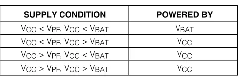
Power Control This function is provided by a temperature-compensat-ed voltage reference and a comparator circuit that
monitors the VCC level. When VCC is greater than VPF,
the part is powered by VCC. When VCCis less than VPF
but greater than VBAT, the DS3231 is powered by VCC.
If VCC is less than VPF and is less than VBAT, the
device is powered by VBAT. See Table 1.
To preserve the battery, the first time VBATis applied to
the device, the oscillator will not start up until VCC is
applied, or until a valid I2C address is written to the
part. Typical oscillator startup time is less than one
sec-ond. Approximately 2 seconds after VCCis applied, or
a valid I2C address is written, the device makes a
tem-perature measurement and applies the calculated cor-rection to the oscillator. Once the oscillator is running, it continues to run as long as a valid power source is
available (VCC or VBAT), and the device continues to
measure the temperature and correct the oscillator fre-quency every 64 seconds.
Pushbutton Reset Function The DS3231 provides for a pushbutton switch to be
con-nected to the RSToutput pin. When the DS3231 is not in
a reset cycle, it continuously monitors the RSTsignal for a low going edge. If an edge transition is detected, the
DS3231 debounces the switch by pulling the RST low.
After the internal timer has expired (PBDB), the DS3231
continues to monitor the RSTline. If the line is still low, the DS3231 continuously monitors the line looking for a rising edge. Upon detecting release, the DS3231 forces the RSTpin low and holds it low for tRST.
The same pin, RST, is used to indicate a power-fail
con-dition. When VCCis lower than VPF, an internal power-fail
signal is generated, which forces the RSTpin low. When
VCCreturns to a level above VPF, the RSTpin is held low
for approximately 250ms (tREC) to allow the power
sup-ply to stabilize. If the oscillator is not running (see the Power Control section) when VCC is applied, tREC is
bypassed and RSTimmediately goes high.
Real-Time Clock With the clock source from the TCXO, the RTC provides seconds, minutes, hours, day, date, month, and year information. The date at the end of the month is automati-cally adjusted for months with fewer than 31 days, includ-ing corrections for leap year. The clock operates in either the 24-hour or 12-hour format with an AM/PM indicator. The clock provides two programmable time-of-day alarms and a programmable square-wave output. The
INT/SQW pin either generates an interrupt due to alarm
condition or outputs a square-wave signal and the selection is controlled by the bit INTCN.
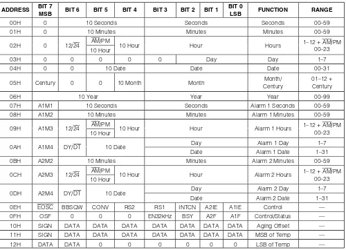
Address Map
Figure 1 shows the address map for the DS3231 time-keeping registers. During a multibyte access, when the address pointer reaches the end of the register space(12h), it wraps around to location 00h. On an I2C
START or address pointer incrementing to location 00h, the current time is transferred to a second set of regis-ters. The time information is read from these secondary registers, while the clock may continue to run. This eliminates the need to reread the registers in case the main registers update during a read.
I
2
C Interface
The I2C interface is accessible whenever either VCC or
VBATis at a valid level. If a microcontroller connected to
the DS3231 resets because of a loss of VCC or other
event, it is possible that the microcontroller and DS3231
I2C communications could become unsynchronized,
e.g., the microcontroller resets while reading data from the DS3231. When the microcontroller resets, the
SUPPLY CONDITION POWERED BY
DS3231 I2C interface may be placed into a known state
by toggling SCL until SDA is observed to be at a high level. At that point the microcontroller should pull SDA low while SCL is high, generating a START condition.
hours). The century bit (bit 7 of the month register) is tog-gled when the years register overflows from 99 to 00. The day-of-week register increments at midnight.
DS3231
Figure 1. Timekeeing Registers
Note: Unless otherwise specified, the registers’ state is not defined when power is first applied.
ADDRESS BIT 7
MSB BIT 6 BIT 5 BIT 4 BIT 3 BIT 2 BIT 1
BIT 0
LSB FUNCTION RANGE
00H 0 10 Seconds Seconds Seconds 00–59
01H 0 10 Minutes Minutes Minutes 00–59
AM/PM
02H 0 12/24
10 Hour 10 Hour Hour Hours
1–12 + AM/PM 00–23
03H 0 0 0 0 0 Day Day 1–7
04H 0 0 10 Date Date Date 00–31
05H Century 0 0 10 Month Month Month/
Century
01–12 + Century
06H 10 Year Year Year 00–99
07H A1M1 10 Seconds Seconds Alarm 1 Seconds 00–59
08H A1M2 10 Minutes Minutes Alarm 1 Minutes 00–59
AM/PM
09H A1M3 12/24
10 Hour 10 Hour Hour Alarm 1 Hours
1–12 + AM/PM 00–23
Day Alarm 1 Day 1–7
0AH A1M4 DY/DT 10 Date
Date Alarm 1 Date 1–31
0BH A2M2 10 Minutes Minutes Alarm 2 Minutes 00–59
AM/PM
0CH A2M3 12/24
10 Hour 10 Hour Hour Alarm 2 Hours
1–12 + AM/PM 00–23
Day Alarm 2 Day 1–7
0DH A2M4 DY/DT 10 Date
Date Alarm 2 Date 1–31
0EH EOSC BBSQW CONV RS2 RS1 INTCN A2IE A1IE Control —
0FH OSF 0 0 0 EN32kHz BSY A2F A1F Control/Status —
10H SIGN DATA DATA DATA DATA DATA DATA DATA Aging Offset —
11H SIGN DATA DATA DATA DATA DATA DATA DATA MSB of Temp —
DS3231
The countdown chain is reset whenever the seconds register is written. Write transfers occur on the acknowl-edge from the DS3231. Once the countdown chain is reset, to avoid rollover issues the remaining time and date registers must be written within 1 second. The 1Hz square-wave output, if enabled, transitions high 500ms after the seconds data transfer, provided the oscillator is already running.
Alarms
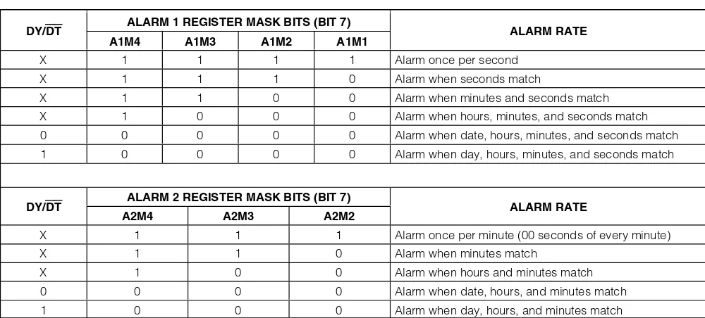
The DS3231 contains two time-of-day/date alarms. Alarm 1 can be set by writing to registers 07h to 0Ah. Alarm 2 can be set by writing to registers 0Bh to 0Dh. The alarms can be programmed (by the alarm enable and INTCN bits of the control register) to activate theINT/SQW output on an alarm match condition. Bit 7 of
each of the time-of-day/date alarm registers are mask bits (Table 2). When all the mask bits for each alarm are logic 0, an alarm only occurs when the values in the timekeeping registers match the corresponding values
stored in the time-of-day/date alarm registers. The alarms can also be programmed to repeat every sec-ond, minute, hour, day, or date. Table 2 shows the pos-sible settings. Configurations not listed in the table will result in illogical operation.
The DY/DT bits (bit 6 of the alarm day/date registers)
control whether the alarm value stored in bits 0 to 5 of that register reflects the day of the week or the date of the month. If DY/DT is written to logic 0, the alarm will be the result of a match with date of the month. If DY/DTis written to logic 1, the alarm will be the result of a match with day of the week.
When the RTC register values match alarm register set-tings, the corresponding Alarm Flag ‘A1F’ or ‘A2F’ bit is set to logic 1. If the corresponding Alarm Interrupt Enable ‘A1IE’ or ‘A2IE’ is also set to logic 1 and the INTCN bit is set to logic 1, the alarm condition will
acti-vate the INT/SQW signal. The match is tested on the
once-per-second update of the time and date registers.
Table 2. Alarm Mask Bits
ALARM 1 REGISTER MASK BITS (BIT 7) DY/DT
A1M4 A1M3 A1M2 A1M1 ALARM RATE
X 1 1 1 1 Alarm once per second
X 1 1 1 0 Alarm when seconds match
X 1 1 0 0 Alarm when minutes and seconds match
X 1 0 0 0 Alarm when hours, minutes, and seconds match
0 0 0 0 0 Alarm when date, hours, minutes, and seconds match
1 0 0 0 0 Alarm when day, hours, minutes, and seconds match
ALARM 2 REGISTER MASK BITS (BIT 7) DY/DT
A2M4 A2M3 A2M2 ALARM RATE
X 1 1 1 Alarm once per minute (00 seconds of every minute)
X 1 1 0 Alarm when minutes match
X 1 0 0 Alarm when hours and minutes match
0 0 0 0 Alarm when date, hours, and minutes match
Special-Purpose Registers
The DS3231 has two additional registers (control and status) that control the real-time clock, alarms, and square-wave output.Control Register (0Eh)
Bit 7: Enable Oscillator (EOSC). When set to logic 0, the oscillator is started. When set to logic 1, the
oscilla-tor is stopped when the DS3231 switches to VBAT. This
bit is clear (logic 0) when power is first applied. When
the DS3231 is powered by VCC, the oscillator is always
on regardless of the status of the EOSCbit.
Bit 6: Battery-Backed Square-Wave Enable (BBSQW). When set to logic 1 and the DS3231 is
being powered by the VBAT pin, this bit enables the
square-wave output when VCC is absent. When
BBSQW is logic 0, the INT/SQW pin goes high
imped-ance when VCC falls below the power-fail trip point.
This bit is disabled (logic 0) when power is first applied.
Bit 5: Convert Temperature (CONV). Setting this bit to 1 forces the temperature sensor to convert the temper-ature into digital code and execute the TCXO algorithm to update the capacitance array to the oscillator. This can only happen during the idle period. The status bit, BSY, prevents the bit from being set when BSY = 1. The user should check the status bit BSY before forcing the controller to start a new TCXO execution. A user-ini-tiated temperature conversion does not affect the inter-nal 64-second update cycle.
A user-initiated temperature conversion does not affect the BSY bit for approximately 2ms. The CONV bit remains at a 1 from the time it is written until the conver-sion is finished, at which time both CONV and BSY go
Bit 2: Interrupt Control (INTCN). This bit controls the
INT/SQW signal. When the INTCN bit is set to logic 0, a
square wave is output on the INT/SQW pin. When the
INTCN bit is set to logic 1, then a match between the timekeeping registers and either of the alarm registers
activates the INT/SQW (if the alarm is also enabled).
The corresponding alarm flag is always set regardless of the state of the INTCN bit. The INTCN bit is set to logic 1 when power is first applied.
Bit 1: Alarm 2 Interrupt Enable (A2IE). When set to logic 1, this bit permits the alarm 2 flag (A2F) bit in the
status register to assert INT/SQW (when INTCN = 1).
When the A2IE bit is set to logic 0 or INTCN is set to logic 0, the A2F bit does not initiate an interrupt signal. The A2IE bit is disabled (logic 0) when power is first applied.
Bit 0: Alarm 1 Interrupt Enable (A1IE). When set to logic 1, this bit permits the alarm 1 flag (A1F) bit in the
status register to assert INT/SQW (when INTCN = 1).
When the A1IE bit is set to logic 0 or INTCN is set to
logic 0, the A1F bit does not initiate the INT/SQW
sig-nal. The A1IE bit is disabled (logic 0) when power is first applied.
DS3231
BIT 7 BIT 6 BIT 5 BIT 4 BIT 3 BIT 2 BIT 1 BIT 0
EOSC BBSQW CONV RS2 RS1 INTCN A2IE A1IE
RS2 RS1 SQUARE-WAVE OUTPUT
FREQUENCY
0 0 1Hz
0 1 1.024kHz
1 0 4.096kHz
1 1 8.192kHz
SQUARE-WAVE OUTPUT FREQUENCY
DS3231
Status Register (0Fh)Bit 7: Oscillator Stop Flag (OSF). A logic 1 in this bit indicates that the oscillator either is stopped or was stopped for some period and may be used to judge the validity of the timekeeping data. This bit is set to logic 1 any time that the oscillator stops. The following are examples of conditions that can cause the OSF bit to be set:
1) The first time power is applied.
2) The voltages present on both VCC and VBAT are
insufficient to support oscillation.
3) The EOSCbit is turned off in battery-backed mode.
4) External influences on the crystal (i.e., noise, leak-age, etc.).
This bit remains at logic 1 until written to logic 0.
Bit 3: Enable 32kHz Output (EN32kHz).This bit indi-cates the status of the 32kHz pin. When set to logic 1, the 32kHz pin is enabled and outputs a 32.768kHz square-wave signal. When set to logic 0, the 32kHz pin goes to a high-impedance state. The initial power-up state of this bit is logic 1, and a 32.768kHz square-wave signal appears at the 32kHz pin after a power source is applied to the DS3231 (if the oscillator is running).
Bit 2: Busy (BSY).This bit indicates the device is busy executing TCXO functions. It goes to logic 1 when the conversion signal to the temperature sensor is asserted and then is cleared when the device is in the 1-minute idle state.
Bit 1: Alarm 2 Flag (A2F).A logic 1 in the alarm 2 flag bit indicates that the time matched the alarm 2 regis-ters. If the A2IE bit is logic 1 and the INTCN bit is set to
logic 1, the INT/SQW pin is also asserted. A2F is
cleared when written to logic 0. This bit can only be written to logic 0. Attempting to write to logic 1 leaves the value unchanged.
Bit 0: Alarm 1 Flag (A1F).A logic 1 in the alarm 1 flag bit indicates that the time matched the alarm 1 regis-ters. If the A1IE bit is logic 1 and the INTCN bit is set to
logic 1, the INT/SQW pin is also asserted. A1F is
cleared when written to logic 0. This bit can only be written to logic 0. Attempting to write to logic 1 leaves the value unchanged.
Crystal Aging
The crystal aging offset register provides an 8-bit code to add to the codes in the capacitance array registers. The code is encoded in two’s complement. One LSB represents one small capacitor to be switched in or out of the capacitance array at the crystal pins. The offset register is added to the capacitance array register under the following conditions: during a normal temper-ature conversion, if the tempertemper-ature changes from the previous conversion, or during a manual user conver-sion (setting the CONV bit). To see the effects of the aging register on the 32kHz output frequency immedi-ately, a manual conversion should be started after each aging register change.Positive aging values add capacitance to the array, slowing the oscillator frequency. Negative values remove capacitance from the array, increasing the oscillator frequency.
The change in ppm per LSB is different at different tem-peratures. The frequency vs. temperature curve is shift-ed by the values usshift-ed in this register. At +25°C, one LSB typically provides about 0.1ppm change in frequency.
BIT 7 BIT 6 BIT 5 BIT 4 BIT 3 BIT 2 BIT 1 BIT 0
Sign Data Data Data Data Data Data Data
Crystal Aging Offset (10h)
BIT 7 BIT 6 BIT 5 BIT 4 BIT 3 BIT 2 BIT 1 BIT 0
OSF 0 0 0 EN32kHz BSY A2F A1F
Temperature Registers (11h–12h)
Temperature is represented as a 10-bit code with a res-olution of +0.25°C and is accessible at location 11h and 12h. The temperature is encoded in two’s comple-ment format. The upper 8 bits are at location 11h and the lower 2 bits are in the upper nibble at location 12h. Upon power reset, the registers are set to a default temperature of 0°C and the controller starts a tempera-ture conversion. New temperatempera-ture readings are stored in this register.I
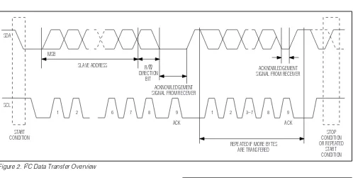
2C Serial Data Bus
The DS3231 supports a bidirectional I2C bus and data
transmission protocol. A device that sends data onto the bus is defined as a transmitter and a device receiv-ing data is defined as a receiver. The device that con-trols the message is called a master. The devices that are controlled by the master are slaves. The bus must be controlled by a master device that generates the serial clock (SCL), controls the bus access, and gener-ates the START and STOP conditions. The DS3231
operates as a slave on the I2C bus. Connections to the
bus are made through the SCL input and open-drain SDA I/O lines. Within the bus specifications, a standard mode (100kHz maximum clock rate) and a fast mode (400kHz maximum clock rate) are defined. The DS3231 works in both modes.
Bus not busy: Both data and clock lines remain high.
Start data transfer: A change in the state of the data line from high to low, while the clock line is high, defines a START condition.
Stop data transfer:A change in the state of the data line from low to high, while the clock line is high, defines a STOP condition.
Data valid: The state of the data line represents valid data when, after a START condition, the data line is stable for the duration of the high period of the clock signal. The data on the line must be changed during the low period of the clock signal. There is one clock pulse per bit of data.
Each data transfer is initiated with a START condition and terminated with a STOP condition. The number of data bytes transferred between the START and the STOP conditions is not limited, and is determined by the master device. The information is transferred byte-wise and each receiver acknowledges with a ninth bit.
Acknowledge: Each receiving device, when addressed, is obliged to generate an acknowledge after the reception of each byte. The master device must generate an extra clock pulse, which is associ-ated with this acknowledge bit.
DS3231
BIT 7 BIT 6 BIT 5 BIT 4 BIT 3 BIT 2 BIT 1 BIT 0
Sign Data Data Data Data Data Data Data
Temperature Register (Upper Byte) (11h)
BIT 7 BIT 6 BIT 5 BIT 4 BIT 3 BIT 2 BIT 1 BIT 0
Data Data 0 0 0 0 0 0
DS3231
Figures 3 and 4 detail how data transfer is
accom-plished on the I2C bus. Depending upon the state of
the R/Wbit, two types of data transfer are possible:
Data transfer from a master transmitter to a slave receiver. The first byte transmitted by the master is the slave address. Next follows a number of data bytes. The slave returns an acknowledge bit after each received byte. Data is transferred with the most significant bit (MSB) first.
Data transfer from a slave transmitter to a master receiver. The first byte (the slave address) is trans-mitted by the master. The slave then returns an acknowledge bit. Next follows a number of data bytes transmitted by the slave to the master. The master returns an acknowledge bit after all received bytes other than the last byte. At the end of the last received byte, a not acknowledge is returned. The master device generates all the serial clock puls-es and the START and STOP conditions. A transfer is ended with a STOP condition or with a repeated START condition. Since a repeated START condition is also the beginning of the next serial transfer, the bus will not be released. Data is transferred with the most significant bit (MSB) first.
The DS3231 can operate in the following two modes:
Slave receiver mode (DS3231 write mode): Serial data and clock are received through SDA and SCL. After each byte is received, an acknowledge bit is transmitted. START and STOP conditions are recog-nized as the beginning and end of a serial transfer.
Address recognition is performed by hardware after reception of the slave address and direction bit. The slave address byte is the first byte received after the master generates the START condition. The slave address byte contains the 7-bit DS3231 address, which is 1101000, followed by the direction bit (R/W), which is 0 for a write. After receiving and decoding the slave address byte, the DS3231 outputs an
STOP CONDITION OR REPEATED
START CONDITION REPEATED IF MORE BYTES
ARE TRANSFERED ACK START CONDITION ACK ACKNOWLEDGEMENT SIGNAL FROM RECEIVER
ACKNOWLEDGEMENT SIGNAL FROM RECEIVER SLAVE ADDRESS MSB SCL SDA R/W DIRECTION BIT
1 2 6 7 8 9 1 2 3–7 8 9
Figure 2. I2C Data Transfer Overview
A XXXXXXXX A
1101000
S 0 XXXXXXXX A XXXXXXXX A XXXXXXXX A P <SLAVE
ADDRESS>
S = START A = ACKNOWLEDGE P = STOP
R/W = READ/WRITE OR DIRECTION BIT ADDRESS = D0H
<RW>
DATA TRANSFERRED (X + 1 BYTES + ACKNOWLEDGE)
<DATA (n + X)> <DATA (n + 1)>
<DATA (n)> <WORD
ADDRESS (n)>
Figure 3. Slave Receiver Mode (Write Mode)
A XXXXXXXX A 1101000
S 1 XXXXXXXX A XXXXXXXX A XXXXXXXX A P <SLAVE
ADDRESS>
S = START A = ACKNOWLEDGE P = STOP
A = NOT ACKNOWLEDGE
R/W = READ/WRITE OR DIRECTION BIT ADDRESS = D1H
<RW>
DATA TRANSFERRED (X + 1 BYTES + ACKNOWLEDGE)
NOTE: LAST DATA BYTE IS FOLLOWED BY A NOT ACKNOWLEDGE (A) SIGNAL
<DATA (n + X)> <DATA (n + 2)>
<DATA (n + 1)> <DATA (n)>
acknowledge on SDA. After the DS3231 acknowl-edges the slave address + write bit, the master transmits a word address to the DS3231. This sets the register pointer on the DS3231, with the DS3231 acknowledging the transfer. The master may then transmit zero or more bytes of data, with the DS3231 acknowledging each byte received. The register pointer increments after each data byte is trans-ferred. The master generates a STOP condition to terminate the data write.
Slave transmitter mode (DS3231 read mode): The first byte is received and handled as in the slave receiver mode. However, in this mode, the direction bit indicates that the transfer direction is reversed. Serial data is transmitted on SDA by the DS3231 while the serial clock is input on SCL. START and STOP conditions are recognized as the beginning and end of a serial transfer. Address recognition is performed by hardware after reception of the slave address and direction bit. The slave address byte is the first byte received after the master generates a START condition. The slave address byte contains the 7-bit DS3231 address, which is 1101000,
fol-lowed by the direction bit (R/W), which is 1 for a
read. After receiving and decoding the slave address byte, the DS3231 outputs an acknowledge on SDA. The DS3231 then begins to transmit data starting with the register address pointed to by the register pointer. If the register pointer is not written to before the initiation of a read mode, the first address that is read is the last one stored in the register point-er. The DS3231 must receive a not acknowledge to end a read.
Handling, PC Board Layout,
and Assembly
The DS3231 package contains a quartz tuning-fork crystal. Pick-and-place equipment can be used, but precautions should be taken to ensure that excessive shocks are avoided. Ultrasonic cleaning should be avoided to prevent damage to the crystal.Avoid running signal traces under the package, unless a ground plane is placed between the package and the signal line. All N.C. (no connect) pins must be connect-ed to ground.
Moisture-sensitive packages are shipped from the facto-ry dfacto-ry packed. Handling instructions listed on the pack-age label must be followed to prevent dampack-age during reflow. See IPC/JEDEC J-STD-020 standard for moisture-sensitive device (MSD) classifications and reflow pro-files. Exposure to reflow is limited to 2 times maximum.
DS3231
Chip Information
TRANSISTOR COUNT: 33,000SUBSTRATE CONNECTED TO GROUND PROCESS: CMOS
Thermal Information
Theta-JA: +73°C/WTheta-JC: +23°C/W
16 15 14 13 12 11 10 9 1
2 3 4 5 6 7 8
32kHz SCL
SDA VBAT
GND N.C. N.C. N.C. N.C. TOP VIEW
SO
VCC
INT/SQW
N.C. RST N.C.
N.C. N.C.
DS3231S
DS3231