Features
2. High-performance, Low-power AVR® 8-bit Microcontroller 3. Advanced RISC Architecture
– 131 Powerful Instructions – Most Single-clock Cycle Execution
– 32 x 8 General Purpose Working Registers
– Fully Static Operation
– Up to 16 MIPS Throughput at 16 MHz
– On-chip 2-cycle Multiplier
4. Nonvolatile Program and Data Memories
– 16K Bytes of In-System Self-Programmable Flash
Endurance: 10,000 Write/Erase Cycles
– Optional Boot Code Section with Independent Lock Bits In-System Programming by On-chip Boot Program True Read-While-Write Operation
– 512 Bytes EEPROM
Endurance: 100,000 Write/Erase Cycles
– 1K Byte Internal SRAM
– Programming Lock for Software Security
4. JTAG (IEEE std. 1149.1 Compliant) Interface
– Boundary-scan Capabilities According to the JTAG Standard
– Extensive On-chip Debug Support
– Programming of Flash, EEPROM, Fuses, and Lock Bits through the JTAG Interface
5. Peripheral Features
– Two 8-bit Timer/Counters with Separate Prescalers and Compare Modes
– Real Time Counter with Separate Oscillator
– Four PWM Channels
– 8-channel, 10-bit ADC
8 Single-ended Channels
7 Differential Channels in TQFP Package Only
2 Differential Channels with Programmable Gain at 1x, 10x, or 200x
– Byte-oriented Two-wire Serial Interface
– Programmable Serial USART
– Master/Slave SPI Serial Interface
– Programmable Watchdog Timer with Separate On-chip Oscillator
– On-chip Analog Comparator
• Special Microcontroller Features
– Power-on Reset and Programmable Brown-out Detection
– Internal Calibrated RC Oscillator
– External and Internal Interrupt Sources
– Six Sleep Modes: Idle, ADC Noise Reduction, Power-save, Power-down, Standby and Extended Standby
• I/O and Packages
– 32 Programmable I/O Lines
– 40-pin PDIP, 44-lead TQFP, and 44-pad MLF
• Operating Voltages
– 2.7 - 5.5V for ATmega16L
• Speed Grades
– 0 - 8 MHz for ATmega16L
– 0 - 16 MHz for ATmega16
The AVR core combines a rich instruction set with 32 general purpose working registers.
All the 32 registers are directly connected to the Arithmetic Logic Unit (ALU), allowing
two independent registers to be accessed in one single instruction executed in one clock
cycle. The resulting architecture is more code efficient while achieving throughputs up to
ten times faster than conventional CISC microcontrollers.
The ATmega16 provides the following features: 16K bytes of In-System Programmable
Flash Program memory with Read-While-Write capabilities, 512 bytes EEPROM, 1K
byte SRAM, 32 general purpose I/O lines, 32 general purpose working registers, a
JTAG interface for Boundary-scan, On-chip Debugging support and programming, three
flexible Timer/Counters with compare modes, Internal and External Interrupts, a serial
programmable USART, a byte oriented Two-wire Serial Interface, an 8-channel, 10-bit
ADC with optional differential input stage with programmable gain (TQFP package only),
a programmable Watchdog Timer with Internal Oscillator, an SPI serial port, and six
software selectable power saving modes. The Idle mode stops the CPU while allowing
the USART, Two-wire interface, A/D Converter, SRAM, Timer/Counters, SPI port, and
interrupt system to continue functioning. The Power-down mode saves the register con-
tents but freezes the Oscillator, disabling all other chip functions until the next External
continues
to run, allowing the user to maintain a timer base while the rest of the device is sleeping.
The ADC Noise Reduction mode stops the CPU and all I/O modules except Asynchro-
nous Timer and ADC, to minimize switching noise during ADC conversions. In Standby
mode, the crystal/resonator Oscillator is running while the rest of the device is sleeping.
This allows very fast start-up combined with low-power consumption. In Extended
Standby mode, both the main Oscillator and the Asynchronous Timer continue to run.
The device is manufactured using Atmel’s high density nonvolatile memory
technology.
The On-chip ISP Flash allows the program memory to be reprogrammed in-system
through an SPI serial interface, by a conventional nonvolatile memory programmer, or
by an On-chip Boot program running on the AVR core. The boot program can use any
interface to download the application program in the Application Flash memory. Soft-
ware in the Boot Flash section will continue to run while the Application Flash section is
updated, providing true Read-While-Write operation. By combining an 8-bit RISC CPU
with In-System Self-Programmable Flash on a monolithic chip, the Atmel ATmega16 is
a powerful microcontroller that provides a highly-flexible and cost-effective solution to
many embedded control applications.
The ATmega16 AVR is supported with a full suite of program and system development
tools including: C compilers, macro assemblers, program debugger/simulators, in-circuit
emulators, and evaluation kits.
Digital supply voltage. Ground.
Port A serves as the analog inputs to the A/D Converter.
Port A also serves as an 8-bit bi-directional I/O port, if the A/D Converter is not used.
Port pins can provide internal pull-up resistors (selected for each bit). The Port A output
buffers have symmetrical drive characteristics with both high sink and source capability.
When pins PA0 to PA7 are used as inputs and are externally pulled low, they will source
current if the internal pull-up resistors are activated. The Port A pins are tri-stated when
3. Block Diagram of the AVR MCU Architecture
Data Bus 8-bit
Flash
Program Status
Counter and Control
Program
Control Lines Comparator
I/O Module1
In order to maximize performance and parallelism, the AVR uses a Harvard architecture
The fast-access Register file contains 32 x 8-bit general purpose working registers with a single clock cycle access time. This allows single-cycle Arithmetic Logic Unit (ALU) operation. In a typical ALU operation, two operands are output from the Register file, the operation is executed, and the result is stored back in the Register file – in one clock cycle.
Six of the 32 registers can be used as three 16-bit indirect address register pointers for Data Space addressing – enabling efficient address calculations. One of the these address pointers can also be used as an address pointer for look up tables in Flash Pro-gram memory. These added function registers are the 16-bit X-, Y-, and Z-register, described later in this section.
The ALU supports arithmetic and logic operations between registers or between a con-stant and a register. Single register operations can also be executed in the ALU.
This section describes the general access timing concepts for instruction execution. The AVR CPU is driven by the CPU clock clkCPU, directly generated from the selected clock source for the chip. No internal clock division is used.
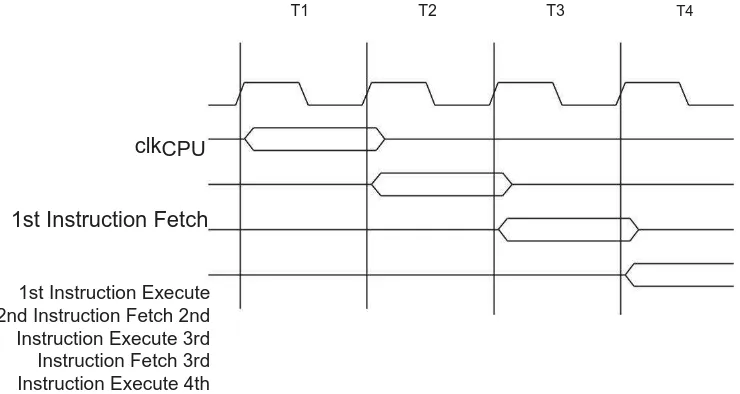
Figure 6 shows the parallel instruction fetches and instruction executions enabled by the Harvard architecture and the fast-access Register file concept. This is the basic pipelin-ing concept to obtain up to 1 MIPS per MHz with the corresponding unique results for functions per cost, functions per clocks, and functions per power-unit.
Figure 6.The Parallel Instruction Fetches and Instruction Executions
T1 T2 T3 T4
clkCPU
1st Instruction Fetch
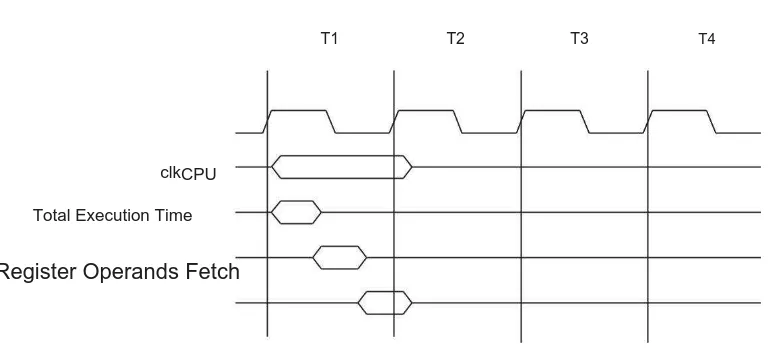
Figure 7 shows the internal timing concept for the Register file. In a single clock cycle an ALU operation using two register operands is executed, and the result is stored back to the destination register.
Figure 7.Single Cycle ALU Operation
T1 T2 T3 T4
clkCPU
Total Execution Time
Register Operands Fetch
ALU Operation Execute
Result Write Back
The AVR provides several different interrupt sources. These interrupts and the separate reset vector each have a separate program vector in the program memory space. All interrupts are assigned individual enable bits which must be written logic one together with the Global Interrupt Enable bit in the Status Register in order to enable the interrupt. Depending on the program counter value, interrupts may be automatically disabled when Boot Lock bits BLB02 or BLB12 are programmed. This feature improves software security. See the section
“Memory Programming” on page 254 for details.
The lowest addresses in the program memory space are by default defined as the Reset and Interrupt Vectors. The complete list of vectors is shown in “Interrupts” on page 42. The list also determines the priority levels of the different interrupts. The lower the address the higher is the priority level. RESET has the highest priority, and next is INT0
The EEPROM Write Enable Signal EEWE is the write strobe to the EEPROM. When address and data are correctly set up, the EEWE bit must be written to one to write the value into the EEPROM. The EEMWE bit must be written to one before a logical one is written to EEWE, otherwise no EEPROM write takes place. The following procedure should be followed when writing the EEPROM (the order of steps 3 and 4 is not essential):
1. Wait until EEWE becomes zero.
2. Wait until SPMEN in SPMCR becomes writing a zero to EEWE in EECR.
6. Within four clock cycles after setting EEMWE, write a logical one to EEWE.
The EEPROM can not be programmed during a CPU write to the Flash memory. The software must check that the Flash programming is completed before initiating a new EEPROM write. Step 2 is only relevant if the software contains a Boot Loader allowing the CPU to program the Flash. If the Flash is never being updated by the
CPU, step 2 can be omitted. See “Boot Loader
Support – Read-While-Write Self-Programming” on page 241 for details about boot programming.
When the write access time has elapsed, the EEWE bit is cleared by hardware. The user software can poll this bit and wait for a zero before writing the next byte. When EEWE has been set, the CPU is halted for two cycles before the next instruction is executed.
• Bit 0 – EERE: EEPROM Read Enable cycles before the next instruction is executed.
The user should poll the EEWE bit before starting the read operation. If a write operation is in progress, it is neither possible to read the EEPROM, nor to change the EEAR register.
The calibrated Oscillator is used to time the
3 x 4 Keypad Module
merupakan suatu modul keypadberukuran 3 kolom x 4 baris. Modul ini dapat difungsikan sebagai input dalam aplikasi seperti pengaman digital, datalogger, absensi, pengendali kecepatan motor, robotik, dan sebagainya.1.Memiliki 12 tombol (fungsi tombol tergantung aplikasi).
2.Memiliki konfigurasi 4 baris (input scanning) dan 3 kolom (output scanning).
3.Kompatibel penuh dengan DT-51™ Low Cost Series dan DT-AVR Low Cost Series. Mendukung DT-51™ Minimum System (MinSys) ver 3.0, DT-51™ PetraFuz, DT-BASIC Series, dan lain-lain.
Alokasi Pin J3
R4
R3
R2
R1
NC
C3
C2
C1
VCC
NC
2
NC = tidak terhubung ke mana-mana
Cx = kolom ke-x Rx = baris ke-x
Contoh Koneksi
Pada dasarnya pin Cx dan Rx pada J3 bebas dihubungkan ke pin input/output manapun pada mikrokontroler. Koneksi berikut ini hanya contoh dan tidak mutlak.
DT-51™ Low Cost Series DT-I/O 3x4
dan DT-AVR Low Cost Series Keypad Module
VCC (Pin 2 PORT1) atau