Utilizing Leveling Techniques in DDR3 SDRAM Memory Interfaces
Introduction
The DDR3 SDRAM memory architectures support higher bandwidths with bus rates of 600 Mbps to 1.6 Gbps (300 to 800 MHz), 1.5V operation for lower power, and higher densities of 2 Gbits on a 90-nm process. While this
architecture is undoubtedly faster, larger, and lower power per bit, just how does one go about interfacing a DDR3 SDRAM DIMM to an FPGA? Leveling is the key word. Without having the leveling feature built directly into the FPGA I/O structure, interfacing anything to a DDR3 SDRAM DIMM is going to be complicated, costly, and involve numerous external components. So, what is leveling and why is it so important?
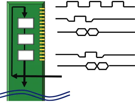
In order to improve signal integrity for supporting higher performance, JEDEC defined fly-by termination for clocks and the command/address bus. This fly-by topology reduces the simultaneous switching noise (SSN) but causes flight-time skew between clock and data/strobes at every DRAM as the clock and address/command signals traverse the DIMM, as shown in Figure 1.
Figure 1. DDR3 SDRAM DIMMs: Flight-Time Skew Reduces SSN, Data Must Be Levelled up to 2 Clock Cycles at the Controller
This flight time skew can be up to 0.8 tCK, enough spread not to know which of two clock cycles the data may return in. Therefore, the “leveling” feature was defined for DDR3 memories by JEDEC to enable controllers to compensate for this skew by adjusting the timing per byte lane.
The latest FPGAs offer many features that interface with double data rate SDRAM memories for a wide range of applications such as desktops, servers, storage, LCD displays, and networking and communication equipment. However, to work with the newest DRAM technology, DDR3 SDRAM, a robust leveling scheme is required.
FPGA I/O Structure
FPGAs, such as the recently announced Altera® Stratix® III device family, provide I/Os capable of high speeds and
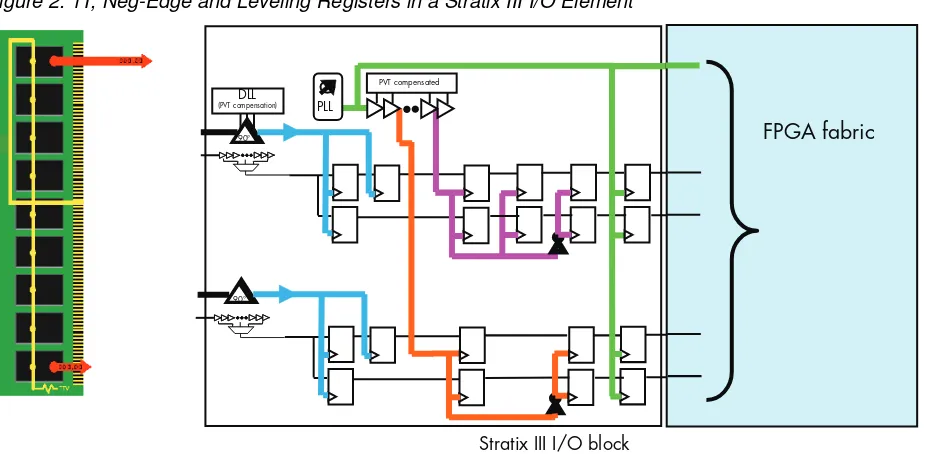
Figure 2. 1T, Neg-Edge and Leveling Registers in a Stratix III I/O Element
Initially, each separate DQS is phase-shifted a nominal 90 degrees and the DQ data associated with its group is captured. Then a free-running resynchronization clock (at the same frequency and phase of the DQS) is used to move the data from its capture domain into the leveling circuit—shown by the pink and orange links in Figure 2. At this stage, each DQS group has a separate resynchronization clock.
Next the DQ data is passed to the 1T registers. Figure 2 shows an example of the 1T register being required in the upper channel to delay the DQ data bits in that particular DQS group. Note that in this example, the 1T registers are not required in the lower channel. This process begins aligning the upper channel to the lower channel. Whether the 1T registers are required or not for any given channel is decided automatically as part of the calibration scheme in free PHY IP core.
Both DQS groups are then passed on the neg-edge registers. Again, optional registers are switched in or out at start up by the automatic calibration process, if required. The final stage is to align both the upper and lower channels back onto the same resynchronization clock, thus creating a source synchronous interface that passes a fully aligned, or levelled, single data rate (SDR) data to the FPGA fabric.
Write Leveling
Similar to read leveling but in reverse, DQS groups are launched at separate times to coincide with a clock arriving at devices on the DIMM, and must meet the tDQSS parameters of +/- 0.25 tCK.
Other FPGA I/O Innovations
High-end FPGAs have a host of other innovative I/O features that allow simple and robust interfacing to a range of memory interfaces such as dynamic on-chip termination (OCT), variable I/O delay, and half data rate (HDR) capability, as shown in Figure 3. This remainder of this paper follows these features (from left to right), pausing at each step to examine each in detail.
Figure 3. Useful I/O Features for DDR3 SDRAM Memory Interfaces
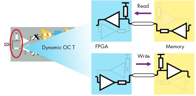
Dynamic OCT
Parallel and serial OCT provide the appropriate line termination and impedance matching for both the read and write busses. This removes the need for external resistors at the FPGA and saves on external component costs, board space, and routing complexity. It also significantly reduces power consumption, because the parallel termination is
effectively out of circuit on a write operation. Figure 4 shows the terminations for both read and write operations.
Figure 4. Dynamic OCT - Read and Write Operations
Variable Delay for DQ Deskew
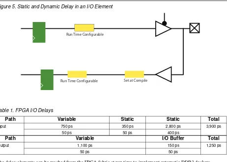
Variable input and output delay (shown in Figure 5) can be used for trace length mismatch and electrical deskew. The fine input and output delay resolution (i.e., 50-picosecond (ps) steps) can be used for finer inter-DQS deskew (separate to the leveling function) caused either by mismatch in board length or variations in I/O buffers of the FPGA and memory devices, as demonstrated in Table 1. Ultimately, this increases the capture margin for each DQS group.
Write
FPGA Memory
Read
Figure 5. Static and Dynamic Delay in an I/O Element
The delay elements can be reached from the FPGA fabric at run time to implement automatic DDR3 deskew algorithms as part of the start-up calibration process. Figure 6 shows an illustration of how DQ data can be deskewed and centered around DQS for extra capture margin. The output delay can also be used to insert a small amount of skew into the output path to intentionally reduce the number of I/Os being switched simultaneously.
Figure 6. Conceptual DQ Deskew Within a DQS Group Centered Around 90-Degree Phase-Shifted DQS
Reliable Capture
The DQS signals act as the input strobes and must be shifted to an optimal position for capture of read transactions. The phase-shift circuitry (shown in Figure 7) can shift the incoming DQS signals by 0°, 22.5°, 30°, 36°, 45°, 60°, Table 1. FPGA I/O Delays
Path Variable Static Static Total
Input 750 ps 350 ps 2,800 ps 3,900 ps
50 ps 50 ps 400 ps
Path Variable I/O Buffer Total
Output 1,100 ps 150 ps 1,250 ps
50 ps 50 ps
Run Time Configurable
Run Time Configurable Set at Compile
Figure 7. DQ Capture Circuit
The delay-locked loop (DLL) shown in Figure 7 maintains the phase shift in a fixed location across PVT. Figure 8
shows the relationship between the DLL and phase-shift circuitry.
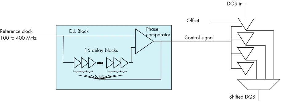
Figure 8. DLL and DQS Phase-Shift Circuitry
The DLL uses a frequency reference to generate control signals dynamically for the delay chains in each of the DQS pins, allowing it to compensate for PVT variations. There are four DLLs in a Stratix III device, each located in a corner of the device. Each DLL can reach two sides of the device, allowing support for multiple DDR3 SDRAM memory interfaces on all sides of the device.
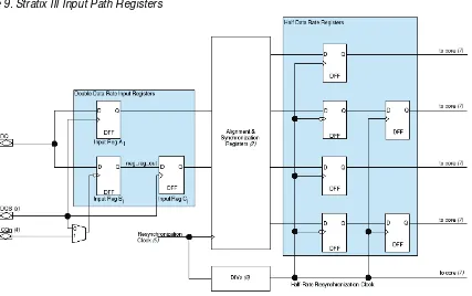
High-Speed Data Rate Domain Crossing and Design Simplification
DDR capture registers and HDR registers allow safe transfer of data from the double data rate domain (data on both edges of the clock), down to the SDR domain (data on single positive edge of clock at the same frequency, but at twice the data width), down to HDR domain (data on the positive edge of clock, but the frequency is now half that of the SDR and the data width is again doubled), making the internal design timing much easier to achieve. Figure 9
shows how the DQ data moves through these various data rate domains.
Control signal Offset
DQS in
Shifted DQS Phase
comparator Reference clock
100 to 400 MHz
DLL Block
Figure 9. Stratix III Input Path Registers
Die, Package, and Digital Signal Integrity Enhancements
The design of an FPGA die and package should provide robust signal integrity for the high-performance memory interfaces (i.e., having an 8:1:1 user I/O to ground and power ratio and optimized signal return paths as shown in
Figure 10). In addition, the design should provide OCT, variable slew rate, and programmable drive strength to correctly manage signal quality.
Figure 10. Eight User I/Os to Each Power and Ground