Circuits and Systems for Wireless
Communications
Edited by
Markus Helfenstein
and
George S. Moschytz
Swiss Federal Institute of Technology, Zurich
Print ISBN: 0-792-3
-©2002 Kluwer Academic Publishers
New York, Boston, Dordrecht, London, Moscow
All rights reserved
No part of this eBook may be reproduced or transmitted in any form or by any means, electronic, mechanical, recording, or otherwise, without written consent from the Publisher
Created in the United States of America
Preface
Part I RF System Integration
1
RF System Integration
Chris Toumazou
1.1 Introduction to the following papers
References
2
RF System Board Level Integration for Mobile Phones
Gordon J. Aspin Transmitter noise in the receiver band Receiver blocking vs. sensitivity
Integration of RF Systems on a Chip
29
Towards the Full Integration of Wireless Front-End Circuits
Michiel Steyaert
GSM Transceiver Front-End Circuits in 0.25 µm CMOS
Qiuting Huang, Paolo Orsatti, and Francesco Piazza
5.1 5.2 5.3
Introduction
Transceiver architecture and relevant GSM specifications Low-noise amplifier
Part II RF Front-End Circuits
6
RF Front-End Circuits Qiuting Huang
6.1 Introduction to the following papers
7
Phase-Noise-to-Carrier Ratio in LC Oscillators
Qiuting Huang
77 7.2 The weaknesses of existing phase noise models
7.2.1
7.2.2
7.2.3
7.2.4
Linear, frequency-domain analyses with noise sources additive to the carrier signal
Linear frequency domain analyses with noise sources additive to the phase of the carrier
Time-domain analyses with noise sources additive to the carrier signal
Time domain analyses with noise sources additive to the phase of the carrier
General description of LC oscillator operation and determina-tion of oscilladetermina-tion amplitude
Oscillator response to an interfering current Noise-to-carrier ratio in a CMOS colpitts oscillator Exact design of RF oscillators
Conclusions
References
8
Design Study of a 900 MHz/1.8 GHz CMOS Transceiver for Dual-Band Applications
Mihai Banu, Carlo Samori, Jack Glas, and John Khoury
9.1
Stefan Heinen and Stefan Herzinger
RF Challenges for Tomorrow’s Wireless Terminals
Petteri Alinikula
Part III Wideband Conversion for Software Radio
12
Wideband Conversion for Software Radio
José E. Franca
12.1 Introduction to the following papers
References
13
Wide-band Sub-Sampling A/D Conversion with Image Rejection
C. Azeredo-Leme, Ricardo Reis, and Eduardo Viegas
13.1
Wide-band A/D Conversion for Base Stations
187
Low-Spurious ADC Architectures for Software Radio
Bang-Sup Song
Part IV Process Technologies for Future RF Systems
16
Process Technologies for Future RF Sytsems
Urs Lott
16.1 Introduction to the following papers
17
Low-Cost Si and Si/Si1 _ xGex Heterostructure BiCMOS Technologies for Wireless Applications
Lateral etching and amorphous Si refilling process Si/Si1_rGer heterostructure bipolar transistors 17.4.1
17.4.2
Epitaxial growth and material properties of Si1-xGex Si1-xGex bipolar transistor structures
17.5 Summary
References
18
GaAs-Based RFIC Technology for Consumer Radios
235 Predicting the future: Where are consumer radios going? Low-tech GaAs MESFETs: Cost-effective RF integration Conclusion
19
Monolithic Integrated Transceiver Circuits for GHz Frequencies
Urs Lott and Werner Bächtold
19.1 Some myths about RF integrated circuits
19.1.1 19.1.2 19.1.3 19.1.4
Is using a single technology an advantage? Present technologies for RF integrated circuits Technology choices for baseband circuits
Pros and cons of complete integration 19.2 Examples of GHz transceiver circuits
19.2.1 19.2.2 19.2.3
Low noise amplifiers in the 2 GHz range 5 GHz LNA with switch for antenna diversity 17 GHz PHEMT power amplifier
19.3 Conclusions
References
Part V DSP for Wireless Communications
20
Efficient Design Flow for Fixed-Point Systems
Holger Keding, Martin Coors, and Heinrich Meyr
21.1
Utilisation of statistical knowledge for interpolation 21.5 Back ends
21.5.1 ANSI-C and fast-simulation back end 21.6 Conclusion
279
E. Lambers, C. Moerman, P. Kievits, J. Walkier, and R. Woudsma
22.1
The art of VLSI signal processing Overview on smart antennas
Hardware implementation of the QRD-RLS algorithm Application to temporal reference beamforming
Evolution of Speech Coding for Wireless Communications
Gilles Miet
Variable bit rates for speech and channel codecs Complexity/performance compromise of the AMR
327 25.2 Benchmarks of digital signal processing routines
25.2.1
Evolution of features for DSP implementation General-purpose versus application-specific DSPs 25.3 Conclusion
References
Part VI Blind Channel Equalization
26
Blind Channel Equalization
Ruey-wen Liu
26.1 Introduction to the following papers
References
Channel Estimation and Equalization in Wireless ATM
Lang Tong
28.3 Channel estimation and equalization in wireless ATM 28.3.1 PACE: Protocol-aided channel equalization 28.4 Conclusion
References
29
Blind Separation and Combination of High-Rate QAM Signals
John Treichler, C. R. Johnson, Jr., and S. L Wood
371 372
373
375 29.4
29.5
Performance Conclusions
References
30
This book contains revised contributions by the speakers of the 1st IEEE Workshop on Wireless-Communication Circuits and Systems, held in Lucerne, Switzerland, from June 22–24, 1998. The aim of the workshop was to apply the vast expertise of the CAS Society in the area of circuit and system design to the rapidly growing field of wireless communications. The workshop combined presentations by invited experts from academia and industry with panel and informal discussions. The following topics were covered:
RF System Integration (single-chip systems, CMOS RF circuits),
RF Front-End Circuits (CMOS RF oscillators, broadband design techniques), Wideband Conversion for Software Radio (A/D conversion issues, wideband
sub-sampling, low-spurious A/D conversion),
Process Technologies for Future RF Systems (Si, SiGe, GaAs, CMOS, packaging technologies),
DSP for Wireless Communications (DSP algorithms, fixed-point systems, DSP for baseband applications),
Blind Channel Equalization (adaptive interference suppression, design techniques, channel estimation).
The workshop was a great success, with over 130 participants from 19 countries, from the U.S. to Europe and Asia, including a large contingent of participants from industry (60 %). Feedback from the participants showed that the carefully selected combination of tutorial-like lectures with lectures on specialized and advanced topics was a feature of the workshop that was particularly appreciated. Due to the relatively strong involvement of industry — both in the form of lecturers and listeners — a high level of discussion was attained in both panel sessions and informal gatherings.
By a stroke of luck, Philips Semiconductors, Zurich, Switzerland, celebrated their 50th anniversary in 1998. With the well-deserved spirit of celebration and generos-ity that this anniversary triggered at Philips, and the goodwill and encouragement of the Board of Governors and Excom members of the CAS Society, the finances were guaranteed at an early stage. For this the organizers were very grateful.
The format of this workshop and book has strongly been influenced by the AACD workshop series organized by J. H. Huijsing, R. J. van de Plassche and W. Sansen. The editors greatly appreciate the inspiration provided by this series.
It is a pleasure to acknowledge the speakers and authors for making available their expertise. Our sincerest thanks go also to D. Arnold, M. Goldenberg, D. F. Lus-tenberger, H. Mathis, and H. P. Schmid for helping in the preparation of the workshop and book. Moreover, D. H. Mathis and H. P. Schmid were strongly involved in the technical editing of this book, which the editors very gratefully acknowledge.
1
RF SYSTEM INTEGRATION
Chris Toumazou
Dept. Elect. & Electron. Eng. Imperial College Exhibition Rd. London SW7 2BT, U.K.
1.1 INTRODUCTION TO THE FOLLOWING PAPERS
The idea for this part of the book arose from a need to convey the intricacies of RF system integration in today’s wireless information system arena. The proliferation of portable communication devices has created a high demand for small and inexpensive transceivers with low power consumption. The Radio-Frequency (RF) and wireless-communications market has suddenly expanded to unimaginable dimensions. Sources predict that mobile telephony subscriptions will increase to over 350 Million in the year 2000.
While this trend continues and challenges still exist, the RF practice at present is one which requires the so-called “green fingers” of design. System integration from the interconnection of sub-blocks at the front-end to the interconnection of metal lay-ers within the IC is all highly interactive. However, what has now become apparent at the low-GHz frequency band is that as feature sizes of silicon devices shrink, there is a more natural move towards VLSI at high frequencies where lumped circuit design is beginning to find a new home. As we start integrating more of the board-level com-ponents onto a single chip, the board layout will then also form a major part of the “lumped” circuit.
Part I has brought together key engineers from industry and academia to shed light on performance demands, board level design, and sub-micron silicon CMOS solutions, taking the reader through realistic design scenarios for RF system integration.
Devices and systems, such as pagers, cellular and cordless phones, cable modems,
mobile faxes, PDAs (Personal Digital Appliances), wireless LANs, and RF identifica-tion tags are rapidly penetrating all aspects of our lives, evolving from luxury items to indispensable tools. Semiconductor and system companies, small and large, ana-logue and digital, have seen the statistics and are striving to capture their own market share by introducing various RF products. Today’s pocket phones contain more than one million transistors, with only a small fraction operating in the RF range and the rest performing low-frequency “base-band” analogue and digital signal processing. However, the RF section is still the design bottleneck of the entire system.
In contrast to other types of analogue and mixed-signal circuits, RF systems de-mand not only a good understanding of integrated circuits, but also of many areas that are not directly related to integrated circuits.
Most recently, as the industry moves toward higher integration and lower cost, RF and wireless design increasingly demands more “concurrent engineering,” thereby re-quiring IC designers from both industry and academia to combine forces and to have a sufficient and integrated knowledge of all the disciplines [1]. RF circuits must process analogue signals with a wide dynamic range at high frequencies. It is interesting to
note that the signals must be treated as analogue even if the modulation is digital or the amplitude carries no information.
The trade-offs involved in the design of such circuits can be summarised in the “RF design hexagon” shown in Fig. 1.2. While any of the seven parameters trade to some extent, all these parameters are severely constrained by the core parameters, namely the power consumption and supply voltage. It is important to recognise that, while digital circuits directly benefit from advances in IC technologies, RF circuits do not benefit as much. This issue is exacerbated by the fact that RF circuits often require external components—for example, inductors—that are difficult to bring onto the chip even in modern IC processes. RF design techniques are thus becoming highly sensi-tive to device physics, and so analog characterisation of digital VLSI technology is of primary concern. One of the major challenges is implementing RF circuits on ICs instead of PCBs, offering advantages including lower production cost, high functional-ity, small physical size, high reliabilfunctional-ity, and low power requirements. It now becomes very necessary to achieve better co-ordination between the “system design” activity and the “RF circuit design” activity.
A few years ago Gallium-Arsenide (GaAs) technology was the primary-choice
semiconductor for implementing RF ICs due to its low noise figure, higher gain and
drive off-chip loads. While integrated silicon BJT transceivers are still more desirable for today’s products, CMOS RF solutions are looking very promising, with the real-istic prospect of a single-chip transceiver in a plastic package. Furthermore, newer device technologies such as Silicon Germanium are maturing rapidly and offer the high mobility necessary for today’s RF wireless products. This array of competing technologies offers system designers more creative opportunity, and the best wireless transceiver solutions may well emerge from system design evolving together with ar-chitecture, circuits, antennas, and power allocation plans. In the future, base-band signal processing will inevitably make up for imperfections in the front end (e.g. soft-ware radio).
Part I begins with a section by Gordon Aspin from TTP Communications, a com-pany with vast experience in RF system integration for cellular products. The section describes the realistic design of a part of a fully integrated transceiver IC from Hitachi which satisfies multi-band GSM RF specifications. Some of the subtleties of board-level integration are presented, coupled with a design approach which attempts to make practical GSM handset design a more straightforward task. Emphasis is placed upon the importance of understanding total system-level requirements when designing a chip, and upon how board level design influences low-level requirements.
In the next section, Peter Mole from Nortel Semiconductors gives an overview of system integration on a chip. Peter takes us through a number of practical RF design is-sues and then discusses general problems that radio systems must overcome to achieve acceptable performance. The section overviews practical concerns for both receiver and transmitter and how different radio architectures can be utilised to overcome some of the problems. The section concludes with a number of practical design issues for integrating radio circuitry in silicon technology.
The final two sections concentrate on the design of fully integrated transceiver chips in sub-micron and deep sub-micron Silicon CMOS technologies. Michiel Steyaert from the Katholieke Universiteit of Leuven introduces us to the arena of using deep sub-micron CMOS to create single-chip transceiver blocks and components such as LNAs, VCOs , up-converters , synthesisers etc. to satisfy cellular performance spec-ifications above 1 GHz. The section discusses all the bottlenecks and challenges of RF CMOS using plain deep sub-micron devices for integration within systems such as DECT, GSM, and DCS 1800.
Finally, Qiuting Huang et. al. from the Integrated Systems Laboratory at ETH Zurich presents a practical high-performance GSM transceiver front-end in a 0.25 µm CMOS process. This section concludes Part I by taking the reader through a practical RF system integration example. The work demonstrates that excellent RF performance is feasible with 0.25 µm CMOS, even in terms of the requirements of the super-hetero-dyne architecture. Design for low noise and low power for GSM handsets has been given particular attention.
References
[1]
[2]
B. Razavi, “Challenges in Portable Transceiver Design”, Circuits and Devices Magazine, IEEE 1996..
2
RF SYSTEM BOARD LEVEL
INTEGRATION FOR MOBILE PHONES
Gordon J. Aspin
TTP Communications Ltd. Melbourn Science Park Royston, SG8 6EE, U.K.
Abstract: This paper highlights the importance of system design choices in the development of RF chip sets for cellular mobile phones. By way of example, the design of the BRIGHT family of RF chip sets for GSM is described. Performance results are presented based on these chip sets.
2.1 INTRODUCTION
Traditionally, the RF system represents one of the most difficult challenges for compa-nies developing digital cellular phones, particularly for compacompa-nies with limited devel-opment experience. It is now possible to buy more or less complete baseband-chip-set solutions together with associated software from a number of vendors. However, al-though off-the-shelf radio-chip-set solutions are available, they nevertheless require a significant level of design expertise on the part of the handset designer in order to re-alise a manufacturable product which meets the necessary performance requirements. This paper describes the results of some of our work to meet the challenge of realising an RF chip set which makes designing a GSM mobile phone a straightforward task.
This work, the development of the RF chip set family, has been carried out in collaboration with Hitachi Semiconductor of Japan.
The initial devices were targeted at single-band products — the main GSM market at that time. Even more important commercially, however, has been the emergence of dual-band 900/1800 capability as a key market requirement. Fortunately, the BRIGHT architecture is particularly well suited to multi-band operation, and the latest-genera-tion devices, BRIGHT2, are designed to support this mode.
The objective of the development has been to achieve the maximum level of inte-gration in the radio system, compatible with the objectives of lowest total system cost, lowest part count, and ease of design and manufacture, within the available IC process technology. The approach is a systems approach with the focus upon achieving a de-vice design in which the radio requirements of the whole product are most simply and elegantly met.
2.2 DESIGN APPROACH
What makes RF IC design particularly interesting is that the silicon represents only a small part of the total RF system but can make a very large difference to how easy
or difficult it is to design the rest of the system. It is therefore vital to understand the
total system requirements when designing the chip. It is also important to be able to validate the design at both device and system level. This is achieved by means of a System Evaluation Board — essentially a complete handset—on which all the system performance parameters can be measured and confirmed (Fig. 2.1). Validation of the system is often one of the most expensive parts of the development.
This radio System Evaluation Board is designed to be compatible with Baseband Evaluation Boards used for baseband chip set and protocol software development work. The two boards can be plugged together to emulate complete handset opera-tion. As well as testing in our own laboratories we have even been able to take such a system through “Type Approval” at a GSM test house to verify radio system perfor-mance.
2.3 KEY GSM SYSTEM SPECS
As with all modern radio standards, there are many specification points for GSM that need to be met in order for the radio to conform to the standard. However, a small number of these specification points turn out to be critical to the radio architecture and design.
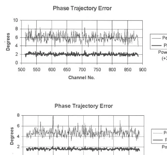
2.3.1 Transmitter phase error
As a digital phase modulation system, GSM controls how closely the transmitted phase follows the ideal modulated phase trajectory. It does this by specifying the phase error in terms of an RMS value (5°) and a peak value (20°), across the useful part of the burst. The phase error is a very critical parameter for the transmitter, because so many things can contribute to it, including digital modulator phase error, synthesiser settling
time, switching transients, I/Q gain and phase imbalance, up-converter phase noise and spurious modulation, and power amplifier AM–to–PM conversion, etc.
In putting together a radio system design, budgets are allocated to each of these parameters. Some, however, can be difficult to quantify theoretically (e.g. switching transients) and may only become apparent once the design is realised in hardware. The task of the system designer is to identify a system architecture in which uncontrollable and unquantifiable effects are minimised.
A classic example of a problematic architecture is the direct-up-converter transmit-ter, in which a baseband I/Q modulator is mixed up to the final frequency in a single stage. As a result, the up-converter’s local oscillator runs also at the final frequency. Maintaining sufficient isolation between the modulated power amplifier output and the unmodulated low-power local oscillator is very difficult, particularly within a minia-ture handset.
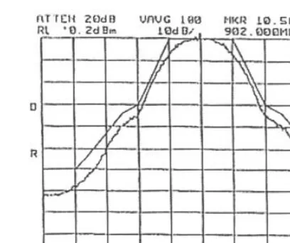
2.3.2 Transmitter modulation spectrum (Fig. 2.2)
Like the phase error, the modulation spectrum is affected by many factors, including digital modulator spectrum, I/Q gain and phase imbalance, up-converter phase noise and spurious modulation, power amplifier AM–to–PM conversion, transmitter noise floor, etc. A good system design will minimise these effects inherently in the design.
2.3.3 Transmitter noise in the receiver band (Fig. 2.3)
In the extended GSM900 band, the specification is relaxed by around 12 dB to
avoid even more severe duplexer filtering requirements. In the 1800MHz bands, the
specifications are comparable to the E-GSM requirements scaled by the frequency.
2.3.4 Receiver blocking vs. sensitivity (Fig. 2.4)
By themselves, neither the receiver blocking nor the receiver sensitivity requirements is intrinsically difficult to meet: it is achieving both requirements simultaneously within a low-power, low-cost handset that is the design challenge. The sensitivity requirements translate into system noise figures of about 10.2 dB at 900 MHz and 12.2 dB at 1800MHz for a typical GSM equaliser realisation. It is good practice to design for a nominal performance at least 4 dB better than these figures to give
ade-quate production margin. The most challenging blocking requirement is the 3 MHz blocking figure which is almost 80 dB up on the wanted signal (74 dB for GSM 1800).
Translated into voltages on chip, it is necessary to receive a signal at a level of around 2 µV, without distortion, in the presence of a blocking signal of around 20 mV. This degree of linearity must be maintained by the receiver front end, i.e. the LNA, and particularly the mixer, before the blocking signal amplitude can be reduced in the first IF filter.
2.4 ARCHITECTURE CHOICES
is the use of an offset phase-locked loop. This approach has substantial benefits for systems like GSM which employ constant envelope modulation.
As a result of the strict phase and modulation accuracy requirements of GSM, it is only really feasible to perform transmit carrier modulation in the digital domain. This must then be converted into an analogue signal and translated to the required transmit frequency. In a conventional approach, the frequency translation is performed in one or more up-conversion stages. One of the problems of trying to do this operation in a single stage, when the mixer’s local oscillator runs at the same frequency as the trans-mitted signal, is that of cross-coupling between the modulated high-level transmitter power output and the unmodulated low-level VCO. A solution to this problem is to use multiple conversions, but each conversion stage introduces spurious conversion prod-ucts which must be filtered out. A better approach is the one illustrated in Fig. 2.5. In this scheme, the required signal modulation is impressed upon a VCO by means of a phase locked loop. The modulated VCO output is mixed down to a suitable interme-diate frequency and compared with the signal from the digital modulator, which has been up-converted to the same IF. The loop comparison frequency is not critical and is chosen to provide a suitable frequency plan. Channelisation is supported by stepping the local oscillator as normal.
The bandwidth of the loop has a significant effect upon overall transmitter perfor-mance. The low-pass filter in the offset PLL must be chosen to optimise the following parameters:
Minimum loop settling time (following frequency steps). Good phase tracking (to give minimum phase error).
Minimum in-band spurii (to meet modulation spectrum requirements).
Suppression of wide-band modulator noise (to meet transmit noise in receive band requirements).
Typically, a loop bandwidth of around 1 MHz is found to be optimum. Using a basic offset PLL design of the form shown has clear benefits:
The noise floor of the VCO is sufficiently low so that it can meet the receiver-band noise-floor requirements without further filtering. The duplex filter can be replaced by a simple low-pass harmonic filter and a transmit/receive switch, with consider-able cost and space savings.
Removing the duplex filter reduces the loss in the transmit path by around 1 dB. This implies up to 25% longer talk time for the handset.
Removing the duplex filter removes a major cause of ripple in the transmit band. This allows the handset manufacturer to make use of the margin in the transmit level specifications to operate the handset closer to the minimum level, thus giving further battery life improvements.
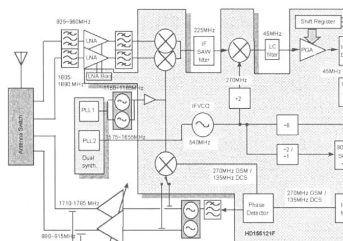
In the receiver, the architectural choice is mainly about the number of conversion stages and the frequency plan. A two-IF approach has been chosen for BRIGHT, with a 225 MHz SAW filter defining the first IF. The use of a relatively high first IF means that image frequencies and other spurious responses from the first mixer cause no particular problems. The majority of receiver gain occurs at the second IF of 45 MHz, and it is here also that the AGC is applied. This approach minimises power consumption in the receiver. In our reference baseband solution (the Analog Devices GSM baseband chip sets), the channel filtering occurs digitally as part of the analogue–to–digital converter—another example of system design choices. Thus, at 45 MHz, only a relatively wide-band LC filter is required to provide protection against blocking of subsequent stages. The architecture of the complete 900 MHz BRIGHT device is shown in Fig. 2.6. The main UHF local oscillator runs at 1150 to 1185 MHz and drives both the receiver first mixer and the transmitter offset mixer. By ensuring that the receiver first IF and the transmitter offset loop comparison frequency are spaced by the Tx/Rx duplex offset (i.e. 45 MHz) the pulling range of the first local oscillator is minimised to the operating bandwidth of 35 MHz.
The loop comparison frequency is chosen to be a multiple of 45 MHz (in this case to give a simple scheme for generating all other required frequencies by on-chip division as shown.
In terms of integration, all the transmit and receive silicon functionality is integrated onto a single device, but the PLL synthesiser functions for the two main oscillators are on a separate device. This choice was based on an assessment of the risk factors in-volved versus the benefits. There is virtually no difference in printed circuit board area whether or not the synthesisers are integrated, yet there is a significant risk of noise in the digital PLL synthesiser leaking into the analogue parts of the chip. Furthermore, the PLL synthesisers are established parts.
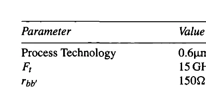
The front-end low noise amplifier is also not fully integrated within the BRIGHT device. Initial studies identified that it would be very difficult to achieve the necessary noise figure and blocking performance from an integrated amplifier. Instead it was decided to integrate the bias function for the LNA, and to use an external transistor as the amplifying device. The final die for the BRIGHT 900 MHz part is shown in Fig. 2.7. Some key process and packaging parameters are summarised in Tab. 2.1.
develop-ment of the BRIGHT2 device. The BRIGHT architecture is well suited to dual-band operation, with only small adaptations. On the receive side, the only change is the inclusion of a second mixer to support the second band: the first IF and subsequent
circuitry is shared between both bands. On the transmit side, the only change is the
inclusion of a different divide ratio for operation at 1800 MHz, giving an offset loop
comparison frequency of 135 MHz. For minimum VCO range, the difference between transmit and receive IFs should equal the Tx/Rx duplex offset. In this case, for the 1800MHz operation, we have a 90 MHz IF separation, compared to a 75 MHz du-plex offset—thus giving around 20% excess pulling requirement over the theoretical minimum.
All other areas of the architecture are essentially unchanged. For market reasons, however, a digital AGC is included in BRIGHT2, compared to the analogue AGC scheme used in the original BRIGHT. It is found that the digital AGC gives better performance than the analogue AGC, because the on-chip DAC can be better matched to the characteristics of the AGC amplifier.
2.5 RESULTS
2.5.1 Transmitter phase error
2.5.2 Transmitter modulation spectrum
2.5.3 Receive sensitivity
Fig. 2.12 shows the measured receive sensitivity in both bands plotted as a function of channel number. For GSM900, the specification is –102 dBm, for GSM1800, the specification is –100dBm. A minimum margin of 4dB is achieved on these figures, with 5–7 dB typical margin. This provides sufficient margin for production and tem-perature tolerances.
2.5.4 Blocking performance
for GSM1800. Around 2–3 dB margin is thus achieved in each band. The blocking performance of BRIGHT2 in the GSM900 band is further illustrated in Fig. 2.14. A wanted signal is applied, 3 dB above the reference sensitivity level, and then the level
of blocking signal which causes the receiver BER to degrade to the nominal 2% level, is measured. The wanted signal is on channel 61, i.e. at 947.2MHz.
The GSM requirements are as follows:
The most difficult requirement is the 3 MHz blocker, and for this, a minimum of 1.5 dB margin is demonstrated. Since these measurements were made, it was iden-tified that the first mixer was not particularly well-matched (hence the ripple), and subsequently better performance with more than 3 dB margin has been demonstrated.
2.6 FUTURE OPTIONS
Looking to the future, there are a number of possible options. Firstly, the levels of inte-gration can be increased, for example by including on chip the VCOs or the baseband interface. The challenge with putting VCOs on chip is to realise circuits of sufficiently high Q to meet the phase noise requirements; also low-loss varactors are not normally realisable in a BiCMOS IC process. Nevertheless, there is much interest in this area.
does not help reduce the total number of pins in the package very much, and the area for a 64-pin QFP is actually greater than for a 48-pin QFP plus a 20-pin SSOP. Also, because the baseband interface may be realised in smaller geometries than the RF device, the total power consumption may be increased by integration.
A more fruitful line is perhaps to consider greater functionality. In this regard, triple-band phones may be a market requirement soon, a requirement which may be supported as a further extension of the BRIGHT architecture.
3
INTEGRATION OF RF SYSTEMS
ON A CHIP
Peter J. Mole
Nortel Networks London Road Harlow, Essex, CM 17 9NA, U.K.
3.1 RF ISSUES
Before considering the details of implementation of an RF system on a chip, it is worth spending some time discussing the problems that any radio system must overcome if to achieve an acceptable performance. The important aspect to remember is that the radio system never operates in isolation. It is not sufficient to think only of the transmitter, the link and the receiver, though many problems lie in this simple chain alone. It is also important to realise that the transmitter can interfere with other links, and a receiver may be unduly sensitive to unwanted, but entirely legitimate, signals.
3.1.1 Receiver concerns
nal and effectively masking it. It is therefore imperative that these signals are heavily filtered before the input to the receiver.
The receiver must respond to any signal in the system band, however, it must also
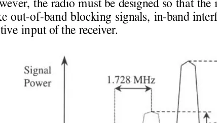
reject unwanted in-band signals without suffering from overload. Such unwanted sig-nals may be significantly larger than the wanted; consider the situation when you are trying to make a cellular phone link to your service provider’s remote base-station but, unfortunately, you are physically adjacent to a second service provider’s base-station. The system specification provides guidelines to the levels of signals which can exist. Fig. 3.1 shows the relative levels for signals in the DECT cordless phone system. In this system, where communication channels are allocated to both time and frequency slots, the frequency channels are separated by 1.728 MHz. A weak signal, (defined in the DECT specification as –73 dBm) must be receivable in the presence of a signal
13 dB stronger in the neighbouring channel and 34 dB stronger in the next neighbour-ing channel. To achieve this rejection of neighbourneighbour-ing interferers, a tunable filter is required. In practice this is achieved by mixing the signal to a fixed intermediate fre-quency and then filtering. The specifications reflect the fact that it is more difficult
to filter the neighbouring channel than more distant ones. Until the signals can be
filtered, however, the radio must be designed so that the interferers do not create over-load. Unlike out-of-band blocking signals, in-band interferers cannot be filtered prior to the sensitive input of the receiver.
The frequency translation that is required in a receiver to move the radio frequency input to the required intermediate frequency for filtering is achieved with a mixer. A mixer effectively multiplies the RF input signal with a chosen local oscillator (LO) signal. Thus we can ideally represent the RF input by and the local oscillator by Thus the output can be written as:
image frequency. It is therefore essential that any signal present at the image frequency
is filtered out in front of the mixer.
In practice, to achieve efficient mixing, it is normal that the LO signal is close to
a square wave. Thus the LO signal will contain the third harmonic of the LO (about 9 dB lower in signal amplitude) which is also multiplied by the input signal. This
immediately means that signals at will also appear at the output as an
intermediate-frequency signal. Other harmonics will behave similarly. Again input signals at these frequencies must be removed prior to mixing.
Another defect of the LO signal is that it suffers from phase noise (or jitter). This means the LO is not a pure tone but a spectrum of signals centred on the desired frequency. Thus the mixer will respond to signals close to the wanted signal with a
sensitivity falling off with the phase-noise spectrum. This problem is known as
recip-rocal mixing. Thus, to ensure that the receiver can reject neighbouring channels, it is important to provide an LO signal with low phase noise. These issues are illustrated in Fig. 3.2.
3.1.2 Transmitter concerns
not constant amplitude. Intermodulation is usually at its worst in the power amplifier itself, but intermodulation throughout the transmitter must be considered.
Broadband noise in the transmitter either due to noise in analogue circuit elements or due to quantisation noise if the signal is generated from a D-to-A converter must be considered. The latter, in particular, will require careful attention to band filtering to ensure low spurious emissions. A low-phase-noise local oscillator is also required to
keep the noise emissions to acceptable levels.
In a mechanism similar to phase noise, spurious signals present on the local oscil-lator will also give rise to spurious emissions on the output signal. Spurious signals can arise from the frequency synthesis process or from unintentional couplings to the VCO. On single-chip systems, the identification of these couplings can be particularly difficult, but attention must be paid to single-ended CMOS input signals which couple strongly to the substrate and also to high-power outputs. An example of the former is given in [1]. These effects are illustrated in Fig. 3.3.
3.2 RADIO ARCHITECTURES
With the issues discussed in the previous section, the advantages of different architec-tures can be discussed both in terms of performance and suitability for integration.
3.2.1 Receiver architectures
The mixer must still handle the complete dynamic range of the in-band signal. After the mixer, a SAW filter can be used to achieve the channel filtering. At these frequencies the SAW filter is small but usually has a large in-band loss when complete channel filtering is to be achieved. The output drive of the mixer must therefore boost the signal level to allow for this loss.
Once the interfering channels have been attenuated, the signal can be boosted to a high level (it can be limited if a constant-amplitude modulation scheme is used). The signal is then reduced to baseband frequency for demodulation. It is of course possible to split the channel filtering between the two intermediate frequencies. This will require a greater dynamic range in the second mixer.
This architecture requires the synthesis of two local oscillators, and their frequen-cies must be chosen so that spurious responses from the radio are kept to a minimum. This aspect of frequency planning, which will not be discussed in more detail here, is a well-understood design process which requires considerable care and experience.
This design requires several external filters and therefore does not lend itself to easy integration as the pin count increases. Moreover, the filters are usually single ended— though this is not essential—and hence achieving isolation between pins becomes an issue. In particular, the channel filter will often need to provide 50 dB of attenuation at key frequencies, thus implying that greater isolation must be achieved between the pins and with respect to signal ground if the filter response is not to be degraded. The image filter can be eliminated if an image-rejecting mixer is used. This will prevent the need to come off chip after the LNA and makes an LNA plus image-reject mixer a useful integrated building block.
The direct-conversion architecture (Fig. 3.5). The direct-conversion receiver, be-cause of its simplicity, appears to offer the best opportunity for integrated systems. Some examples of its use in wireless systems do exist today, but it is not as simple in practice.
baseband filters. Only one local-oscillator frequency needs to be synthesised, and frequency planning is straightforward.
To achieve a precise conversion to baseband, it is important that good quadrature can be achieved at the local-oscillator frequency. Unlike the superheterodyne architec-ture, this quadrature now needs to be achieved at the RF frequency, which poses some problems that are generally soluble.
The main issue is associated with DC signals which are generated by defects in the mixer. These signals are implicitly in-band, it is therefore difficult, and sometimes im-possible, to filter them from the wanted signal. It is necessary to keep them sufficiently below the signal. Unfortunately, the amplification that can be applied to the signal be-fore mixing is limited by the level of in-band interferers which must not overload the mixer.
The DC offsets are caused by a collection of effects. Imbalance in the mixers will lead to a DC output. This is generally a constant quantity and could be cancelled with suitable circuitry. Any leakage of the local oscillator to the input of the receiver will result in a DC signal being generated. If this leakage is via radiation coupling into the antenna, then this may vary with the local environment. Finally, non-linearities in the mixer may cause signals to be generated at DC from other interferers. The latter mech-anisms can be time varying, and any offset cancellation needs to be able to respond to time variation. It is only when special precautions are taken to cancel DC offsets that direct-conversion architectures can be used. More details of the direct-conversion issues are given in [2].
Digitisation at IF (Fig. 3.6). This architecture is still a research activity. After the
can be accommodated will be limited by the number of available bits and the linearity of the converter. It should be noted that a first IF of about 100 MHz will be required to enable adequate image rejection to be obtained at the radio frequency.
If a very-wide-bandwidth A-to-D converter can be used, this system also offers the potential to capture all the activity in the RF band from one receiver. There would be no need to tune to individual channels; this could be done by tuning the digital filter. This would enable radio base-stations to operate on many channels with one radio unit. The number of simultaneous channels that can be received would be limited by the number of DSP filters present.
3.2.2 Transmitter architectures
Direct up-conversion (Fig. 3.7). Direct up-conversion offers a very flexible means
of implementing a general modulation. The baseband I and Q signals contain the phase and amplitude modulation information and can be generated digitally. They are converted to analogue signals using D-to-A converters. The major imperfections of the D-to-A converters are quantisation noise and replications of the wanted signal at multiples of the D-to-A clocking frequency. To prevent spurious emissions at unac-ceptable levels, the signal must be band filtered. The filtering is most easily performed while the signal is at baseband.
To convert the signal to RF, a quadrature up-mix is required. The quality of the quadrature will determine the accuracy of the modulation. Any DC offsets will appear
as a leakage of the local oscillator through to the output. Once there it will appear as
a modulation error. These up-mixer defects must be kept small (about – 40 dBc) in order to obtain a high-integrity communication link. Integration and highly balanced circuitry offer this possibility.
The VCO will be very sensitive to pulling from the output signal as it is operating in the centre of the output band. Whether this architecture is implemented in an inte-grated or a discrete form, unwanted coupling which causes pulling of the VCO will require careful consideration. In integrated form, however, evaluation of the interac-tion between on-chip components is poorly developed. The design uncertainties in this architecture need to be balanced carefully against its undoubted simplicity when considering integration.
Offset up-conversion (Fig. 3.8). In this architecture, the first up-mix is the quadra-ture mix and it is to a low first IF. The lower local-oscillator frequency means that a
good quadrature local oscillator is more easily built and local oscillator feed-through is
less of an issue. As for the direct-conversion architecture, quantisation noise and repli-cations of the signal must be filtered out, though with this architecture the harmonic filter can share this task. The harmonic filter also has the job of removing all the un-wanted mixer products from the first mix to ensure they do not appear as unun-wanted emissions at the output.
The second mixer needs to be a good single-sideband mixer, as the unwanted side-band will be offset from the wanted RF signal by twice the first intermediate frequency and will cause a significant interference problem if not well suppressed. The final mixer can use a quadrature structure to suppress the unwanted sideband, but even with balanced on-chip components some degree of filtering will be required to keep the unwanted image emission low. To achieve this, the unwanted sideband must lie signif-icantly outside the system band, and this will determine the lowest practical limit for the first intermediate frequency.
architec-ture more difficult, but if an external PA is used anyway, this constraint is not severe. The double up-mixer with external harmonic filter is a very useful integrated block.
Loop-locked and modulated VCO (Fig. 3.9). In this architecture the concept is to
reduce the need for signal-path filtering by generating a pure modulated signal from
a VCO. With this concept, since the modulation is effectively applied to the VCO
in-put, amplitude modulation of the signal is not possible. However for phase/frequency modulation schemes this is an attractive option.
To ensure that the modulation is precisely controlled about a desired centre fre-quency, the modulation is applied in a feedback loop. The aim of the loop is to ensure that phase modulation sampled at the VCO output is in exact anti-phase with the phase at the I and Q baseband inputs. This will then result in a constant-phase signal at the phase detector. Using the high-gain phase detector output to drive the VCO, the result-ing loop ensures that this condition is closely maintained. The spurii that can enter the VCO are limited by the bandwidth of the lowpass loop filter, enabling simple control of spurious signals. Because the signal at the PA is very pure, this simplifies the fil-tering after the PA too. Here, only PA generated harmonics need be removed, which requires a lower-loss output filter and hence improved power efficiency.
The absolute frequency is determined by the reference oscillator and the frequency offset/division block. These need to be carefully planned. Offsetting the frequency requires down-mixing, and it is important to filter unwanted products, as for the su-perheterodyne receiver. The frequency planning will however ensure that the VCOs should not be susceptible to pulling, and the main VCO is not susceptible as it is phase coherent with the PA. It is not clear, however, whether for a given frequency require-ment, this architecture can produce a design with low-frequency external filter which is easily integrable.
3.2.3 Architectures overview
integrability due to the need to get signals on and off chip, whilst maintaining good signal and ground isolation.
SAWs are also fixed-performance devices, thus if the radio is required to operate across systems, several filter devices which can be switched into the path will be re-quired. Architectures which will allow the programming of the filters will be very attractive in the future for such multi-mode systems. Architectures where the signal is digitised with a wide dynamic range and is filtered and demodulated using the power and low cost of data processing implemented in a small-dimension CMOS process look attractive for this purpose. However, sufficiently high performance and suffi-ciently low power consumption has not been achieved in the analogue to digital con-version.
Implementation in integrated form offers significant advantages for matched and balanced circuitry. Thus architectures which exploit this, for example image-rejecting mixer based circuits, will evolve as prime candidates for integrated radios. However, in any integrated radio, we need to be able to guarantee isolation between the sections. Currently, isolation is achieved by PCB and screened-compartment design. The move to integration will require that isolation is achieved on chip. At present, design skills in this area are low. The choice of architecture to minimise isolation requirements, and the development of techniques to calculate the isolation across the chip are going to be key factors, if the level of integration of radios is to increase.
3.3 SOME DESIGN ISSUES
In this section, some of the design issues for integrating radio circuitry in silicon tech-nology are introduced.
3.3.1 Power supply and ground coupling
In this circuit, some on-chip capacitance has been added to decouple the power supply. If we assume the power supply is perfectly decoupled close to the chip, then the bond inductance—modified by any mutual coupling between the supply and ground lines—will resonate with the internal decoupling capacitance. If the on-chip circuitry takes a significant current at this resonant frequency (represented by the cur-rent source) then a large power supply ripple will occur. This ripple is limited by the
loss in the circuitry itself and the loss in the decoupling capacitors. Simulation can be used to estimate the magnitude of this ripple and also to decide on the values of the capacitance to use (to put the resonance in an innocuous range) and how much
damping to provide if the circuit does not provide sufficient loss. As general design principles:
Separate power supplies for blocks which require isolation.
Keep ground and power supply pins close to exploit mutual inductance. Add on-chip decoupling, choose resonance away from circuit frequencies. Damp resonance if circuit does not provide sufficient loss.
Try and separate signal grounds and ground power returns if possible.
3.3.2 Substrate coupling
As a general rule, as interconnection and circuitry scales down, cross-talk capacitance decreases. This occurs because the length of interconnect required decreases as the circuit compacts with scaling, whilst the cross-talk capacitance per unit length varies relatively little. This implies that to make higher speed circuitry, all dimensions will
need to be reduced, and integration is a natural route forward.
However, with integration, there is also the possibility that signals will couple through the substrate. With silicon technology, where the substrate is conducting, it is possible for the signal to be conducted through the substrate. Fig. 3.11 illustrates this.
but a good SOI technology will have a low coupling capacitance. The major coupling will be to nearby devices or local contacts. Some of the charge will be injected more deeply and couple to distant circuit elements. This will be a source of interference. Finally, some charge will return via the rear die plate. The die plate potential will vary in response to the charge and the return path impedance (which will include capacitive coupling to other parts of the circuit and the impedance to ground of the die plate). If the die plate does not have a low ground impedance then it can couple the injected signal effectively across the whole chip.
These effects are being studied now. Means of simulation are being developed (for example, see [3]). As a general rule, balanced signals will always help injection, and local grounded substrate contacts are beneficial.
3.3.3 On-chlp oscillators
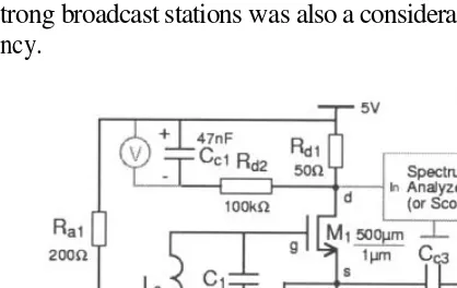
Oscillators on chip always need careful consideration. Although the maintaining am-plifier can be easily accommodated on chip, there is an advantage to keeping the whole oscillator on chip. This however requires an on-chip resonator. The phase-noise per-formance is directly dependent on the resonator’s quality factor. Spiral inductors can be manufactured on chip, but their quality factor is limited by the resistance of the metal used to wind the inductor (losses in the substrate are usually a smaller effect). Measurements of the phase noise achieved using a 2 µm-thick Al/Si/Cu metallisation show that whilst the phase noise required for DECT is attainable, the requirements of a system with much narrower bands such as GSM is rather too demanding.
The second issue to be considered with on-chip oscillators is pulling. The oscil-lator can be considered as a highly shaped and amplified noise source. Essentially, at the resonant frequency, the feedback circuit provides just enough gain to amplify the natural circuit noise to the level required, so this gain is controlled by the limiting mechanism. Away from the natural resonant frequency, the loop gain falls away; the higher the Q the more rapidly the gain falls off. This leads to two defect mechanisms: if a large signal close to resonance couples into the resonator, it will get amplified until it causes the limiter to reduce the gain. The noise content at the output will fall away, and the oscillator will have locked to the interferer. If an interferer is coupled in at a much lower level, then it will not trigger the limiting action; the shaped noise will still exist, but the spurious tone will interact with the oscillations and modulate the frequency. A side-tone will appear at the interferer frequency and a second one on the other side of the main tone—characteristic of FM modulation. Now the sensitivity to such an interferer depends on how close to the main tone the interferer is. If it is at the resonant frequency itself, the coupling only needs to be at circuit noise levels,
the level required increases as the coupling tone is offset in frequency. The higher the
References
[1]
[2]
[3]
Jeff Durec, “An Integrated Silicon Bipolar Receiver Subsystem for 900 MHz ISM Band Application”, JSSCC, vol. 33, Sept. 1998, pp. 1352–1372.
Behzad Razavi, “Design Considerations for Direct Conversion Receivers”, IEEE Transaction on Circuits and Systems-II, Vol. 44, June 1997, pp. 428–435.
4
TOWARDS THE FULL
INTEGRATION OF WIRELESS
FRONT-END CIRCUITS IN
DEEP-SUBMICRON TECHNOLOGIES
Michiel Steyaert
K.U. Leuven, ESAT-MICAS Kardinaal Mercierlaan 94 B–3001 Heverlee, Belgium
Abstract: Research into the potentials of CMOS technologies for RF applications has been growing enormously in the past few years. The trend towards deep sub-micron technologies allows operation frequencies of CMOS circuits above 1 GHz, which opens the way to integrated CMOS RF circuits. Several research groups have developed high performance down-converters, low phase noise voltage-controlled oscillators and dual-modulus pre-scalers in standard CMOS technologies. Research has already resulted in fully integrated receivers and VCO circuits with no external components, neither tuning nor trimming. Further research on low noise amplifiers, up-converters and syn-thesisers has recently resulted in fully integrated CMOS RF transceivers for DCS-1800 applications.
4.1 INTRODUCTION
A few years ago, the world of wireless communications and its applications started to grow rapidly. The driving force for this was the introduction of digital coding and digital signal processing in wireless communications. This digital revolution is driven by the development of high performance, low cost CMOS technologies which allow the integration of an enormous number of digital functions on a single die. This in turn allows the use of sophisticated modulation schemes, complex demodulation algorithms and quality error detection and correction systems, resulting in high-performance, lossless digital communication channels. Low cost and a low power consumption are the driving forces, and they make the analog front-end the bottle neck in future RF designs. Both low cost and low power are closely linked to the trend towards full integration. An ever higher level of integration renders significant space, cost and power reductions. Many different techniques to obtain a higher degree of integration for receivers, transmitters and synthesisers have been presented over the past years [1–3].
Parallel to the trend to further integration, there is the trend to the integration of RF circuitry in CMOS technologies. The mainstream use of CMOS technologies is
the integration of digital circuitry. If possible, using CMOS technologies to integrate
high-performance analog circuits has many benefits. The technology is cheap if used without any special adaptations towards analog design. Plain CMOS has the additional advantage that the performance gap between devices in BiCMOS, nMOS devices in deep sub-micron CMOS, and even NMOS devices in the same BiCMOS process is becoming smaller and smaller due to the much higher investments into the develop-ment of CMOS rather than bipolar technologies. Nowadays, NMOS devices have even higher transition frequencies than NPN devices.
Although some research has been done in the past on the design of RF circuits in CMOS technologies [4], close attention has been given to it only in the past few years [5]. Today, several research groups at universities and in industry are researching this topic [2,3,6,7]. Since bipolar devices are inherently better than CMOS devices, RF CMOS is seen by some people as a possibility for only low performance systems with reduced specifications (like ISM) [8]. Some say that the CMOS processes need adaptations, like substrate etching under inductors. Others feel, however, that the benefits of RF CMOS can be much larger, and that it will be possible to use plain deep sub-micron CMOS for the full integration of transceivers for high performance applications like GSM, DECT and DCS 1800 [2,3].
In this chapter, some trends, limitations and problems in technologies for high fre-quency design are analysed. Second, the down-converter topologies and implemen-tation problems are reviewed. Third, the design and trends towards fully integrated low phase-noise PLL circuits are discussed. Finally, the design of fully integrated up-converters is addressed.
4.2 TECHNOLOGY
deep sub-micron technologies, e.g. transistor lengths of 0.1 µm and below. Transistors whose is near 100 GHz have recently been built in 0.1 µm technologies [9,10].
However, the speed increase of deep sub-micron technologies is reduced by the
par-asitic capacitance of the transistor, meaning the gate-drain overlap capacitances and drain-bulk junction capacitances. This can clearly be seen in Fig. 4.1 in the
compar-ison for different technologies of the and the defined as the 3 dB point of a
diode-connected transistor [11]. The is more important, because it reflects the speed limitation of a transistor in a practical configuration. As can be seen, the rapidly increases, but for real circuit designs the speed improvement is only moderate.
Finally, recent integrations of CMOS RF circuits [5] have made it clear that the limiting factor will not be the technology, but the packaging. Since the RF signals have to come off the chip sooner or later, and since the RF antenna signal has to get into the chip, any parasitic PCB, packaging or bond-wire capacitance in combination with the ESD protection network and packaging pin capacitances will strongly affect and degrade the RF signal.
4.3 FULLY INTEGRATED CMOS DOWN-CONVERTERS
by a signal source). Moreover, in CMOS RF circuit design input and output is becoming a serious problem already in the lower GHz frequency range.
The homodyne or zero-IF receiver has been introduced as an alternative for the IF receiver. It can achieve a much higher degree of integration. The zero-IF receiver
uses a direct, quadrature down-conversion of the wanted signal to the baseband. The wanted signal is its own mirror signal, and sufficient mirror signal suppression can therefore be achieved even with a limited quadrature accuracy. Theoretically, there is thus no discrete high-frequency bandpass filter required in the zero-IF receiver, al-lowing the realisation of a fully integrated receiver, especially if the down-conversion is performed in a single stage (e.g. directly from 900 MHz to the baseband) [6]. The problem of the zero-IF receiver is its poor performance compared to IF-receivers. The zero-IF receiver is intrinsically very sensitive to parasitic baseband signals like DC-offset voltages and crosstalk products caused by RF and LO self-mixing. These draw-backs have kept the zero-IF receiver from being used on a large scale in new wireless applications. The use of the zero-IF receiver has therefore been limited to low-perfor-mance applications like pagers and ISM, in which the coding can be scrambled so that a high-pass filter can be inserted to avoid the DC offset problems. Another application is the use as a second stage in a combined IF/zero-IF receiver topology [12,13]. It
has, however, been shown that with the use of dynamic non-linear DC-correction
algo-rithms implemented in the DSP, the zero-IF topology can be used for high performance applications like GSM and DECT [1,14].
In recent years, new receiver topologies like the low-IF receiver [2,15] were in-troduced for use in high-performance applications. The low-IF receiver performs a down-conversion from the antenna frequency directly down to, as the name already indicates, a low IF (i.e. in the range of a few 100 kHz) [2]. Down-conversion is done in quadrature and the mirror signal suppression is performed at low frequency, af-ter down-conversion, in the DSP. The low-IF receiver is thus closely related with the zero-IF receiver. It can be fully integrated (it does not require an HF mirror signal suppression filter) and uses single stage direct down-conversion. The difference is that the low-IF receiver does not use baseband operation, resulting in a total immunity to parasitic baseband signals, resolving in this way the main disadvantage of the zero-IF receiver. The drawback is that the mirror signal is different from the wanted signal in the low-IF receiver topology, but by carefully choosing the IF frequency, an adja-cent channel with low signal levels can be selected for which the typical mirror signal suppression (i.e. a 3° phase accuracy) is sufficient.
Fig. 4.2 shows the block diagram of a fully integrated quadrature down-converter realised in a 0.7 µm CMOS process [2]. The proposed down-converter does not require any external components, nor does it require any tuning or trimming. It uses a newly developed double-quadrature structure having a very high quadrature accuracy (less than 0.3° in a very large passband). The topology used for the down-converter is based on NMOS transistors in the linear region [2,5]. In combination with capacitors on virtual ground, only a low-frequency opamp is required. Using the MOS transistors in the linear region results in very high linearity for both the RF and the LO input. This
is reflected in a very high third order intercept point (IP3) for the mixers, which is over +45 dBm. The advantages of such a high linearity on both inputs are that the mixer can
4.4 THE SYNTHESISER
The local oscillator is responsible for the correct frequency selection in the up- and down-converters. Since the frequency spectrum in modern wireless communication systems must be used as efficiently as possible, channels are placed together very closely. The signal level of the desired receive channel can be very small, whereas adjacent channels can have very large power levels. Therefore the phase noise
specifi-cations for the LO signal are very hard to meet.
Meanwhile, mobile communication means low power consumption, low cost and low weight. This implies that a completely integrated synthesiser is desirable, where “integrated” means a standard CMOS technology without any external components or processing steps. Usually, the LO is realised as a phase-locked loop. The very hard specs are reflected in the design of the Voltage-Controlled Oscillator (VCO) and the Dual-Modulus Pre-scaler (DMP).
The phase noise of a VCO is one of the most important specifications for telecommunication applications. If there is sideband phase noise at an offset equal to the channel spacing of the system, the down-converter will superimpose the adjacent channel onto the signal in the receive channel. As a result, this will reduce the signal to noise ratio (SNR) of the wanted signal.
the phase noise is inversely related to the power consumption [16].
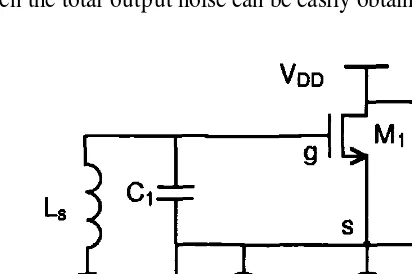
Therefore, the only viable way to obtain a low-power, low-phase-noise VCO is an LC-oscillator with a passive inductor. In this case, the phase noise changes proportion-ally with the power consumption:
As could be expected, the limitation in this oscillator is the integrated passive induc-tor. Equation (4.2) shows that for low phase noise, the resistance R (i.e. the equivalent series resistance in the LC-loop) must be as small as possible. Since the resistance R
will be dominated by the contribution of the inductor’s series resistance, the inductor design is critical. Three solutions exist:
1. Spiral inductors on a silicon substrate usually suffer from high losses in this sub-strate, which limit the obtainable Q-factor. Recently, techniques have been de-veloped to etch this substrate away underneath the spiral coil in a post-processing step [17]. However, since this requires an extra etching step after normal processing of the ICs, this technique is not allowed for mass production.
1 nH/mm and a very low series resistance, very-high-Q inductors can be created. Bondwires are always available in IC technology and can therefore be regarded as being standard CMOS components. Two inductors, formed by four bondwires, can be combined in an enhanced LC-tank to allow a noise/power trade-off [16]. A micro-photograph of the VCO is shown in Fig. 4.3 [18]. The measured phase noise
is as low as –115 dBc/Hz at an offset frequency of 200 kHz from the 1.8-GHz carrier. The power consumption is only 8 mA at 3 V supply. Although chip-to-chip
bonds are used in mass commercial products, they are not characterised on yield performance for mass production. Therefore, the industry is reluctant to accept this solution.
3. The most elegant solution is the use of a spiral coil on a standard silicon substrate without any modifications. Bipolar implementations do not suffer from substrate losses, because they usually have a high-ohmic substrate [19]. Most sub-micron CMOS technologies use a highly doped substrate and have therefore large induced currents in the substrate which are responsible for the high losses [20]. The ef-fects present in these low-ohmic substrates can be investigated with finite-element simulations. This analysis leads to an optimised coil design, which is used in the spiral-inductor LC-oscillator shown in Fig 4.4. Only two metal layers are available, and the substrate is highly doped. With a power consumption as low as 6 mW, a phase noise of – 116dBc/Hz at 600kHz offset from the 1.8-GHz carrier was ob-tained [21].
4.5 RF CMOS UP-CONVERTERS
Until now, mainly CMOS down-conversion mixers have been reported in the open lit-erature. It is only recently that CMOS converters are presented and results are demon-strated [22]. In classical bipolar transceiver implementations, the up- and down-con-verter mixers typically use the same four-quadrant topology. There are, however, some fundamental differences between up- and down-converters, which can be exploited to derive optimal dedicated mixer topologies. In a down-conversion topology, the two input signals are at a high frequency (e.g. 900 MHz for GSM systems) and the output signal is a low-frequency signal of at most a few MHz for low-IF or zero-IF receiver systems. This extra degree of freedom has been used in the design of a very successful down-converter-only CMOS mixer topology [5].
For up-conversion mixers, the situation is totally different. The high-frequency lo-cal oscillator (LO) and the low-frequency baseband (BB) input signal are multiplied to form a high-frequency output signal. All further signal processing has to be performed at high frequencies, which is very difficult and power consuming when using current sub-micron CMOS technologies. Furthermore, all unwanted signals like the intermod-ulation products and LO leakage have to be limited to a level below e.g. –30dB of the signal level.
of CMOS down-converters as well; e.g. in [23] the output signal level is –23 dBm with a LO feed-through signal of –30 dBm, which represents a suppression of only 7 dB. This gives rise to very severe problems in direct up-conversion topologies. The problems above can be overcome in CMOS by linearly modulating the current of a MOS mixing transistor biased in its linear region. For a gate voltage of a drain voltage of and a source voltage of the current through the transistors is given by:
When the LO signal is connected to the gate, and the baseband signal to the current contains frequency components around the LO due to the first term, and com-ponents of the baseband signal due to the second term in equation (4.3), respectively. Based on this principle, a 1 GHz up-converter has been presented in a standard CMOS technology [22] (see Fig. 4.3).