Chapter 10
Digital Integrated Circuits
10 .1 INTRODUCTION
The inte grated circuit (lC)and the digitallogic families were introduced in Section 2.9.This chapter pre sents theelectroniccircuits in each
Ie
digitallog icfamily and analyzestheirelec- trical operatio n. A basicknowledge ofelectricalcircuits isassumed.The
I e
digitallogic families to be consideredhere areRTL D TL TTL E CL
MOS CMOS
Resistor-tran sistorlogic Diode-transistorlogic Transistor-transistorlogic Emitter-coupledlogic Metal -oxide semic onductor
Complementary metal-oxide semiconductor
The firsttwo,RTL and DTL.have only historical significance.since theyareDOlongerused in the design of digital systems .RTL was thefirstcommercialfamilyto havebeen used ex- tensively.Itis included here becau se itrepresentsa use ful starting point for explainingthe basic operationof digital gates.DTL circui ts havebeen replacedbyTILIn fact, TIl.is a modificationofthe DTL gate.The operation of the TI1.. gatewillbeeasier 10undersundafter the DTLgate isanalyzed.TI1..,ECl,andCMOShavea large numbc:rofSSIcircuits,as well asMSl,lSI,and VLSIcompo ne nts.
The basiccircuitin each
Ie
digitallogic familyisaNAND or NOR gate.Thisbasiccircuit is the primary buildingblockfrom whichallother,morecompudigi!al(l'.'O'COlSucobtained.EachIClogic family has adata book that listsallthe integratedcin::uitsiDIbatfamily. Thedif- ferencesin thelogic functionsavailable from each family areDOt10mucbiDtbc:functionsthat
471
472 Chapter10 Digi talIntegrated Circuits
theyachieve asin thespecific electricalcharacteristicsof thebasic gatefrom whichthecircuit is constructed.
NAND and KORgatesareusuallydefined bytheBooleanfunctionsthatthey implement interms ofbinary variables.Inanalyzing themaselectronic circuits.itisneces'illrytoinve s- tigate theirinput-outputrelationshipsintermsoftwo voltagelevels:aIIighle vel.designated byH.andalawlevel,designatedbyL.Asmentioned in Section2.8.theassignmentofbinary 1 toHresults in a positivelogic system and theassignment of binary 1toLresultsin a nega- tivelogic system.Thetruthtable,intermsofHandL,ofa positive-logic r-;'t\..-...;"Dgateisshe ....n inFig.10.1.Wenoticethatthe outputofthegate ishighaslongasoneormore inputsarelow.
The outputis low only when both inputsare high.The behaviorofa positive-logic NA-SD gatein term s of high and lowsignalscan bestatedasfollows:
Ifanyinput of aNANDgate islow.theoutputishigh.
Ifall inputs of aNANDgate arehigh.the outputislow.
Thecorrespondingtruthtablefor a positive-logic:-':ORgateis shown inFig.10.2.The output ofthe NORgateislowwhen oneor moreinputsarehigh.The outputishighwhenbothinputs arelow. Thebehaviorofapositive-logicNORgate, in termsofhighand low signals.canbe statedasfollows:
Ifany inputof aNORgate ishigh.theoutputis low.
Ifall inputs of aNORgate are low,theoutputishigh.
These statementsfor NANDandNORgatesmustberemembered.becausethey willbe u...ed duringtheanalysis of theelectronic gatesin thischapter,
Inputs Output
.,
yz
I. L II
I. II 1/
1/ L II
1/ II L
FIGUR£10.1
Positive-log icNAND gate
Inputs Output
r j' z
I. L 1/
I. 1/ L
1/ L L
1/ 1/ L
FIGUR£ 10 .2
Positive-log icNORgate
10 .2
Section 10.2 Specia l Characterist ics 473
Abipolu rjunrtion rrenstsror(B lT)canbeeither annpllor apup junction transistor.incon- rrast.thefield-effecttransistor (FET)is said tobe unipolar.Theoper ationof a bipolartran- sistor depend s on the now oftwo types of carriers:electrons and holes.The opera tionof a unipola r transistordepends on theflow of onlyonetypeof majority carrier, whichmaybeelec- trons (inann-channel tran sistor ) or holes(ina p-channel transistor ).The first fourdigital logic fam ilies listed at thebegi nning of thechapter-c-Rf'L,DTl,TTL, andEC l- use bipo- lartransistors.Thelasttwo families- MOSand CMOS--employ atype ofunipolartransis- torcalledameral-oxide-serniconductorfield-effe cttransistor. abbrevia ted MOSFET.orMOS forshort.
Inthis chapter. we first introduce the most common characte risticsby which the digi tal logicfam ilies arecompare d. We thendescribe the properties of thebipolar transistorand an- alyzethebasic gates in thebipo lar logic families.Finally. weexplain theoperatio nof the MOS transistor and introdu cethe basic gatesof its two logic families.
SPECIAL CHARACTERISTICS
The charac teris tics of
Ie
digital logicfamili es are usually compared byanalyzing thecircuit of the basic gate in each fam ily. Themost import ant parameters that are evaluatedandcom- pared arefan-out,powerdissipation,propagat ion dela y,and noise margin.Wefirstexplain the properties ofthese parameters and then use them to compare theIe
logic families.Thefan-outof a gate specifies the number of sta ndardloadsthatcan beconne ctedtotheout- put of the gatewithout degrading its norma loperation.Astandardload isusually defined as the amountofcurrent neededby an inputofanother gale in thesamelogic family.Some- timestheterm loadingis usedinstead offan-out.The term is derivedfrom the factthat the outputofa gatecansupplya limited amount ofcurre nt. above which itceasesto operate properly and is said10 beoverloaded. The output of agateis usually connectedtothe inputs ofothergates. Each input requir es a certainamountofcurrentfromthegateoutpu t,so thai eachadditionalconnection adds totheloadofthe gate.loadingrules aresometimesspeci- fiedfora familyof digitalcircuits.Theserules give themaximumamountofloadingallowed for each output of each circuit inthe family. Exceeding thespecified maximum load may causeamalfunc tionbecausethecirc uitcannotsupply thepowerdemanded of it byitsloads.
The fan-out is the maximumnum ber ofinputsthat canbeconnec ted totheoutput ofa gale and isexpressedbyanumber.
Thefan-outis calculated fromthe amountofcurrentavai lable intheoutputofagate and the amount of current neededin eachinput of agale. Consider the cooncdionssOOwnin Fig.10.3.
The outputof one gateis connectedtoone ormore inputsofother
pres.
1beOUtpulofthegale isinthe high-voltag elevel in Fig.1O.3(a ).It provide sacurrentsourceIOHco allthegatein- puts connectedtoit. Each gale inputrequiresa currentlINforproperoperation_Similarly,the outputofthegate isin the low-voltagelevel in Fig. 1O.3(b ).ItprovidesacurrentsinkIOLfor all the gate inputs connected toit.Each gale inputsuppliesacurrenll,L_'Thefan--oul:of megale474 Chapte r10
Digita l Integrate d
Circuits 10•-
J ,.
-
To other inputs (a ) High-level output
I"
Toother inputs (b) Low-level output FIGURll0.J
Fan-c ut computation
is calculate dfromtheratioIOH1IlHorIodIn ,whicheverissmaller.Forexam ple.thestandard TILgateshavethefollowing values forthe currents:
IOH= 400p.A IlH = 40 p.A
IOL = 16mA
In = I.6mA
Thetwo ratiosgive the same numberinthis case:
c
4"OO,-,,,,,A:.:= 16rnA = 10 40p.A 1.6rnATherefore.thefan-outofstandardTILis10.This means thai the output of aTILBatecanbe connected10no more than 10inputs ofother gatesinthe samelogic family.Otherwise.the gale may notbeabletodrive or sinktheamountof currentneededfrom the inputsthat are connected 10 it.
Pow e r Dissipation
Every electroniccircuit requiresa certainamountof power to operate.Thepowerdissipation isaparameter expressedin milliwatts (mW)andrepresentsthe amountofpowerneeded by the gate.Thenumber thatrepresents thisparameter doesnot includethe power deliveredfrom an- othergale;rather.it represents the powerdelivered 10the gate from thepowersupply. An Ie with fourgateswill require.from itspowersupply,fourtimesthe powerdissipated in each gate.
Section 10.2 SpecialCharacteristics 475 The amo unt ofpowerthatisdissipate d inagateis calculatedfrom thesupply voltage Vee and the curre ntIccthatisdrawn by the circuit. Thepower istheproductVee x lee.The cur- rent drain from the powersupply depends on the logicstateofthe gate. The currentdrawn from the power supply when theoutputof the gate is in the high-voltage level istermed ICCH' When theoutput is in the low-voltagelevel,thecurrent istccc The average current is
I ( ) lCCH
+
ICCLcc avg = 2
andis used tocalculate theaveragepower dissipation:
PD(avg) = lcd avg) x V
ce
For example, a standardTTL NANDgate uses a supply voltageVccof 5 V andhas current drainsICCH = IrnA andICCL = 3 rnA.Theaverage currentis (3
+
l)/2 = 2 rnA.The av- erage power dissipationis5 x 2 = 10 mW.AnIe
that has four NAN Dgates dissipates a totalof 10x 4 = 40 mW.In a typical digitalsystem,therewill be many ICs. andthe power requiredbyeachonemustbeconsidered. The totalpower dissipationin the systemis thesum total of the power dissipate din all theICs.Propagation Delay
The propagationdelayof a gateisthe averagetransition-delay time forthe signaltopropagate frominput to output whenthebinary inputsignal changes invalue. Thesignalsthrough a gate take a certain amount of timeto propagatefrom theinputs tothe output. Thisintervaloftime is defined as the propagation delayofthe gate. Propagationdelayis measuredinnanoseconds (ns); Insis equalto 10-9second.
The signals that travel from the inputsofadigitalcircuitto itsoutputs pass throughase- ries of gates.Thesum of thepropagation delaysthrough the gates isthe totaldelay of the cir- cuit.Whenspeedof operationisimportant, each gatemusthave a short propagationdelay and thedigital circuit must havea minimum number ofgates betweeninputs and outputs.
The average propagation delaytime of a gateis calculatedfrom the input and outp utwave- forms,assho wnin Fig.lOA.Thesignal-delaytime between the inputand the output whenthe output changes from the high tothelow levelisreferred to asrnn-Similarly, whenthe out- put goesfromthe low to the highlevel,thedelayistPLH' Itis customarytomeasurethe time between the50 percentpointon the inputand output transitions.Ingeneral.thetwodelays are notthe same,andboth willvary withloadingconditions.TbeaveragepropagaUoo-delay time is calculatedasthe average of thetwodelays.
Asan example.the del ays for a standard TfLgate are t,.HL = 7 nsand t,.LH = II us.
Thesequantitiesare givenintheTfLdatabook. andare measuredwith.loadresiswx::eof 400 ohmsand a loadcapacitanceof 15pF.1be averagepropagatioDdelay01theTIl.pteis
(11
+
7)/2 ~ 9ns.
Under certainconditions.it is more imponamtoknow"themnjnvmdellytimI:ata gaterather than the averagevalue.TheTILdatabookliststhefoUowiDg",Alli n _ prnpIgJ'iondelaysfora standardNANDgate:tPHL
=
15nsandInn = 22ns..
Wbcnspccdofq:cr isaitical.itis necessaryto takeinto account themaximum delayto ensureproperopec 01thecircuiL476 Chapter 10 Digital Integrated Circuits
Input
Output
1 /
/
'\
I \.
" 1 \.'-- _
_ __ I Time
1/
/
- If'LH ~
FIGURE 10.4
Me asure men t of propaga t ion delay
Theinputsignalsinmostdigitalcircuits are appliedsimulta neouslytomorethanonegate.
Allthegates that are connectedto externalinputsconstitute the firstlogi clevelofthecircuit.
Gatesthat receiveatleast one input froman outputofafirst-le....elgateare considered to be in the second logiclevel. andsimilarly for the thirdand higher logiclevels.Thetotalpropa- gatio n del ay ofthecircuit is eq ual to the propagat iondela y ofa gate times the num berof logiclevelsin thecircu it.Thus,a reduction in the number of logiclevels resultsin areduc- tion insig nal delayand faster circuits. Thereductionin thepropagationdelay incircuitsmay bemore im portant than the reduction inthe tota l numberofgales ifspeedofoperationisa maj or factor.
N o ise Margin
Spuriouselectri calsignals from industrial andothersourcescaninduceundesirable voltages ontheconnecting wires between logiccircuits.These unwanted signalsare referred to as notse.Therearetwo type sof noise. DC noiseis caused bya drift in thevoltagelevelsofa signal.ACnoiseis arandom pulsethatmaybecreatedby otherswitchingsignals.Thus.noise is atermused todenotean undesirab le signalthat is superimpos ed uponthe normal operat- ing signal. Thenoisemarginisthemaximumnoise voltage added toan inputsignalofa dig- ital circuitthat doe s nOIcausean undesirable change inthe circuit's outp ut. The ability of circuits tooperate reliably inanenvironme ntwith noise isimport ant in manyapplicatio ns.
Noise marginisexpressed involts and representsthe maximumnoi sesignal that can be tol- erated bythe gate.
The noi se marginis calculated from knowledgeof the voltagesignalavailableintheout- putof {he gateand {hevoltage signalrequired in the inputof the gate.Figure 10.5 illustrates thesignalsusedincomputing the noisemargin.Pan(a ) showsthe rangeofoutputvoltages that canoccurina typical gale.Any voltagein thegate output betweenVeeandVOHisconsidered 10 be thehigh-level state,andany voltagebetween 0 andVOLinthegate outputis consideredto bethe low-levelslat e.Voltages betwee n VOL and VOH are indeterminate anddo nOI appear
Section 10.3 Bipol ar -Transistor Characteristics 477
High-state noisemargin
(b)Inpu t voltagerange
j
Low -stall:
noise margin
===""" 0
(a)Output voltagerange FIGURE 10.5
Signals forevaluat ing noisemargin
undernormal operatingconditions. exceptduring transition bet weenthetwolevels.The cor- respondingtwo voltage rangesthatarerecog nized by the inputofthe gate are indicated in Fig .1O.5(b ).In order tocompensate foranynoise signal.thecircuit mustbe designedso that
V/L isgreaterthan VOLandV/H is lessthanVOH'Thenoisemargin is thedifferenceVOH - V'H
orV/L - VOL ,whichever issmaller.
Asillustratedin Fig.10.5,VOListhe maximum voltagethat theoutputcanbein thelow-level state .The circuitcantolerate anynoi se signal that islessthan the noisemargin (ViI. -
V od
be- cause theinput will recogniz e thesignalasbeing in thelow-level state.Any signal greaterthanVOLplusthenoise-marginfigure willsendtheinputvoltage into theindeterminaterange.which may cause an errorin theoutputofthegate.In a similarfashion , anegauve-volragenoise greater thanVOH - VI H willsendthe input voltageintothe inde terminate range.
The parameters forthe noi se margin ina standa rd TTLNAND gate are VOH = 2.4V,
VOL
=
0.4 V,VI H=
2 V. andVII.=
0.8V.The high-stalenoisemarginis2.4 - 2=
0.4 V,and the low-statenoise marginis0.8 - 0.4 = 0.4V.In this case. beth valuesarethesame.
10 . 3 B I PO LAR - T RA N SI ST O R C H AR A CT ERI STICS
This section reviewsthe bipolartransistor asapplied10digitalcin:uib.. "Ihc iofoIlcwioI.peesemed willbeused in theanalysis ofthebasic circuitinthefour bipolarlogic:farnilieLAsmentioned earlier, bipolar transisto rsmaybeof the npnorpnptype.MOft'O¥'er". (bey~coosttul.Udeither withgermanium orsiliconsemiconductor material.Bipolar
Ie
baiiIii1us.bowe\rcr.are made withsilicon andare usually of the npntype. ....478 Chapter 10 Digital Integrated Circuits
The basic data needed in theanalysisof digitalcircuitsmay be obtainedbyinspection of thetypical characteristiccurvesof acommon-emitternpnsilicontransistor, shown in Fig. 10.6.
Thecircuitin(a) is asimpleinverterwithtwo resistorsand atransistor.The currentmarked IeflowsthroughresistorRcand the collectorofthe transistor. Curren!Isflowsthroughresistor RBand the base of the transistor.The emitter is connected to gro und. and its current 1£ = Ie
+
te-The supplyvoltage isbetween Veeandground. The inputis between V; and ground,andtheoutput isbetweenVoand ground.Wehave assumedpositive direction s for the currentsas indicated.These are thedirections in whichthecurrentsnormallyflow in an npn transistor.Collector and basecurrents(Ieand IB'respectively)are positive whentheyflow intothe transistor.Emitter current
IE
ispositive whenit flowsoutof the transistor.asindicatedbythe arrow in the emitter terminal.Thesym- bol Ve
£ standsfor the voltage drop fromcollector to emitterand is always positive. Corre- spondingly.VB£isthevoltage drop acrossthebase-to-em itterjunction.Thisjunctionis forward biased when VB£ ispositive and reversebiasedwhenVs
£isnegative.lc
~
ReC
v ,
-
R.1. BII,
I.
(rnA)
0.6 0.7
(a) Commonemitterinvertercircuit
I, (rnA)
__ - - -0.6
Vee "...
R, ~ OO
II.-~,--_-
0 .4
11.-_~,-0.4
1I::====':s;:::~ I~ '~ '~ IO.2
rnAr:
Vc£ (V )(b)Tra nsistor-base cha racte ristic fiGURE 10.6
SlIleon npntransist o r characteristics
(c)Transistor-collect or characteristic
Section 10.3 B ipolar-Transist or Characteristics 479
The base-emitter graph icalcharacteristic is shown in Fig.1O.6(b).which is aplot ofVBEver- sus lB'Ifthe base-emittervoltage islessthan 0.6Y,thetran sistoris saidtobecutoffandno base currentflows.When thebase-emitterjunct ion isforward biasedwitha voltagegreaterthan 0.6V.the transistorconductsandIestartsrisingve ry fastwherea sVBEcha nges verylittle.The voltageVBEacross a conducting transistor seldomexceeds0.8V.
The graphical collector-emittercharacteris tics .toge the r with the load line, are shown in Fig.1O.6(c).WhenVBEislessthan 0.6V,thetransistor iscut off with IB = 0,andanegligi - ble current flow s in thecollector. Thecollector-to-emitter circuit then behaves like anopen cir- cuit. With
lc = °
thedrop acrossR e
is0andV o = v e e -
The output isthensaid to bepulled up.Intheactiveregion , coll ectorvoltage VCEmaybeanywhere from about0.8VuptoVec. CollectorcurrentIe inthisregioncanbecalcu latedtobeapproximately equal to18 hFE,where hF£isa transistorparam e tercalledthedecurrelllgain."Themaximum collectorcurre ntdepends not on IB' but ratheronthe extern al circuitconnected to the collector.Thisisbecause VeE is always positiveand itslowest possiblevalue isa v.
For example,in the invertershown,
themax-
imum tcisobtained by makingVeE = 0,toobtain lc = Vee!Re.
The parameterhFEvaries widely over the operatin grangeof the transistor.butstill, it isuse- ful to employ
an
average value forthepurpose ofanalysis.Ina typicaloperat ingrange.hFE isabout50.but undercertainconditionsitcould beas lowas20.Itmustbereali zed that the basecurre ntIBmaybeincreased toanydesirable value,butthe collectorcurre nt Ieislimited byexterna lcircuitparameters.Asa conseque nce. asituationcan be reac hed inwhichhFEIB is greate r thantc.
lfthi scondition exists ,the n the transistoris said to bein the saturationre- gion .Thus,thecondition for saturation is determinedfromthe relationshipIE:2:: Ics
h"
whe retcsisthemaximumcollectorcurre nt flowingduringsaturation.VeEisnot exac tlyzero in thesaturationregion.but isnormallyabo ut0.2 V.In thiscondi tion.Vo= V8E= 0.2Vand theoutput is saidtobepulleddown.
The basicdata needed foranalyzing bipolar-tran sistor digita l circuitsare listedinTable 10.1.
In the cutoff region, VEEislessthan0.6V.VCEis conside red to be an opencircuit, andboth currents are negligible. In the active region,VEEis abo ut0.7V,VeEma y vary ove rawide range,andI
c
canbecalculatedas afunctionoflB'In the saturation region.VBEhardl y changes, butVee dropsto0.2 V.The base currentmustbelargeenou ghtosa tisfy the inequality listed.To simplify the analysis. we will assume that VBE = 0.7V if the transistoris conducting.
whetherin theacti veorsaturation region.
Tab le 10.1
Typicalnp n Siffcon Tronsbtor Paronwten Regi on
Cutoff Active Saturation
<0.6 0.6-0.7 0.7-0.8
Opencircuit
>0.8 02
Current leI.tIonshlp J. z 1c "" O
Ie
= Ia,EI.I. :i!:: laIA'E
480 Chapter 10 Digit alIntegrated Circui ts
Digitalcircuitsmaybeanalyzedbymeans of thefollowingprescribed procedure:Foreach transistorin thecircuit.determinewhether itsVBEislessthan 0.6V.Ifso.then the trans istor is cut off and the collector-to-emittercircuit
is
considere danopencircuit.If\'BEisgreater than 0.6V.the transistormay be intheacti veorsaturationregion.Calculatethebasecurrent.assum ingthat VBE = 0.7 V. Next.calculate the maximum possiblevalue of collector curren t Ics-assumingthatVCE= 0.2V.Thesecalculations willbe interms ofvoltagesappliedand resistorvalues.Then.if thebase current is largeenoughthat18 ~ IcslhFE•we inferthatthe transistorisinthe saturationregionwithVCE = 0.2 V.However.if thebase currentissmaller and the precedingrelat ion ship is not satisfied. thetransistor is in the active regionandwe recalcul atecollectorcurrentlc.usingthe equatio ntc = hFEI8.
Todemon strate withanexample. consider theinverter circuitof Fig. 1O.6I'a)with thefol- lowin gparameters:
Re= I kO RB= 22kO liFE= 50
Vee = 5 V(voltage supply) H = 5 V(high-levelvoltage)
L = 0.2 V(low-levelvoltage)
With input voltageYj = L
=
0.2 V. wehaveVHE-c
0.6Vand thetransistor isCUIoff.The collect or-emittercircuitbehaveslike anopencircuit.sooutput voltageVo=
5 V = H.Withinpu tvoltage Yj = H
=
5 V. we inferthat VSf:>
0.6 V.Assum ingthatV8e = 0.7.wecalculatethe base curre nt:
V; -
V8E 18=
R =B
5 - 0.7
22 kO = 0.195rnA The maximumcollector current.assumingthatVei: = 0.2V. is
Vee- Vee
tcs
= =R e
5 - 0.2
I
to
= 4.8mA0.195 =
Wethenchec kforsaturation.usingthecondition
tcs
4.818
e
hFE = 50 = 0.096mA
whereupo n we find thatthe inequality issatisfied.since 0.195
>
0.096.Weconcludethat the transistoris saturatedand outputvoltageVo = VCE=
0.2 V=
L.Thus.thecircuitbehavesas aninverter.Theproced urejustdescribedwillbeused exten sivelyduring theanalysis ofthe circuitsin the sectionsthat follow.We will performaquathanveanalysis-thatis.ananalysisthat does not involve thespeci fic numericaleq uatio ns.Aquantitativeanalysisandspeci ficcalculations willbeleftas exercises in the "Pro blems" section at theendofthe chapter.
Thereare occasions when no! onlytransisto rs.but alsodiodes.areused in digitalcirc uits.
An
Ie
diodeisusuallyconstructed from a transisto rwithitscollectorconnect ed10 [hebase. as shownin Fig. 1O.7(a).The graphicsymbolem ploye d for adiode is shownin Fig. 1O.7(b ).Thediode behavesessentially like the base-emit terjunct ion ofa tra nsistor. Itsgraphical
Section 10.4 RTlan d OTl Circuit s 481
(a)Transistor ad ap ted for
U~ a~adiode
10 + ~ 02
V.
(b)Diode graphicsymbol
'.
(rnA)
0.6 0.7 (c) Diode ch aracte ristic
1 0.4
FIGURE 10.7
smccndiode symbol andcharact erist ic
characteri stic.shownin Fig. 10.7(c),is similar 10the base-emiucrcharacte risticof atransis- tor.Wecanthen concl udethata diodeis offand nonconductingwhenits forward voltage V
o
is lessthan0.6V.When thediodeconducts. currem lo flowsinthe direction shown in Fig. 1O.7(b )and Vostays atabout0.7V.One mustalways pro vide an extern alresistorto limitthecurrentinacond uct ing diod e.sinceitsvoltageremains fairly constant ata fraction of a \'011.RTl AND DTl CIRCUITS
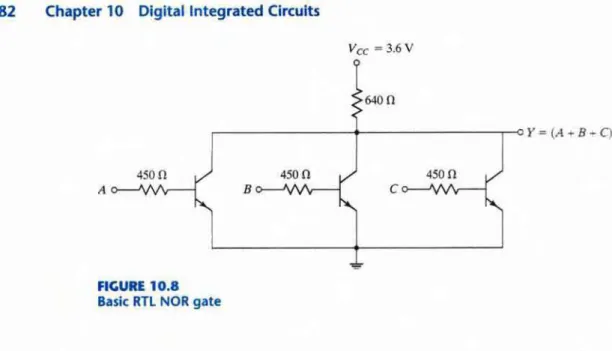
Rn Basic Gate
The basiccircuitof the RTLdigitallogic familyis the NORgateshowninFig. 10.8.Each inputis assoc iated withoneresistorand onetransistor.Thecollectorsofthe transistorsare tied togetherattheoutput.Thevoltagelevelsforthecircu itare0.2V forthelow leveland from I 103.6V forthe highlevel.
Theanalysisofthc RFlcgateis simple andfollows theprocedure outlined intheprevioussec- tion.If any inpu toftheRTLgateishigh,thecorres pondinguan..,istor-isdriven into saturation and theoutputgoeslow,regardles softhe statesoftheother transistors,If all inpu lS are low at 0.2 V,alltransistorsarecutoffbecauseVSE
<
D,6V and the0lllJU ofthecircuilgoeshigh.approachingthevalue of thesupply vo ltageVee,This con firmslhec:ondilionsSUledin Fig.10,2 for the NORgale.Note that thenoisemargin for lowsignalinputis0.6 - D.2= D.4V.
The fan-outoftheRTLgate is limitedbya highOUtpul voltage. A5 die outputisloaded with inputsofothergates.morecurrent isconsumedbytheload..1bi:sCWICIIl must flowthrough the&W-U resistor.Asimplecalculation(seeProblem 10.2) shows
_if"FE
drops to 20.the output voltagedropstoabout IVwhenthefan-outisS.Any\IOItagebelow 1Vin theoutpul482 Chap ter 10 Digital Inte gra ted Circuits
Vcc- 3.6V
6400
r---+---,.~y. (A. B· C)'
4500 4500
FIGURE 10.8 BasicRTL NOR gate
maynot drivethe nexttransistorinto saturationasrequired.The powerdissipation oftheRTL gate is about 12
m w
and thepropagationdelayaverages25 ns.DTL Basic Gates
Thebasic circuit intheOTL digitallogic familyisthe NANDgateshowninFig.10.9.Each input isassociated withone diode.Thediodes and the 5·k O resistorfonn an AXOgate.The transistor servesasacurrent amplifierwhileinvertingthedigitalsignal.The twovoltagelev- els are 0.2Vforthe lowleveland between4 and 5Vforthehighlevel.
The analysisof theDTLgateshouldconform to theconditions listedin Fig.10.1 forthe NANDgate.Ifany inputof the gale islowat 0.2V.the corresponding inputdiode conducts
Y- (ABC)'
n
I 2k SkO
~ DI D2
V
QIP SkO
"'
B A
C
FIGURE 10.9
BasicOTL NAND gate
Section 10.4 RTL and OTL Circuits 483
currentthroughVeeand the5-kfl resistor into the input node.The voltage atpointPis equal 10 theinputvoltage of 0.2V plusadiode drop of 0.7V,for a total of 0.9V.In order for thetran- siste r to startconducting, thevoltage at pointPmustovercome(i.e.,be atleast as highas)a I· VBEdropinQJplustwo diodedropsacrossDI andD2,or3 X 0.6 = 1.8 V.Since the volt- age atPismaintained at 0.9V by the inputconductingdiode.thetransistor is cut off with no drop acrossthe 2-kO resistor.andthe outputvoltage ishigh at5 V.
Ifall inputsof the gate are high,thetransistorisdriven into the saturation region.The vo lt age at P no w is equal to VBE plus the two diode drops across DI and D2, or 0.7 X3 = 2.1 V.Since all inputsare high at 5 V andsinceVp = 2.1V,the inputdiodes are reverse biased and off.The base current is equal to the differenceofthe currentsflowinginthe
IWO5·kn resistorsand is sufficient to drivethetransistorinto saturation.(SeeProblem10.3.) With thetransistor saturated,the output drops toVa = 0.2 V,whichisthe low levelfor the gate.
Thepowerdissipation of aDIL gateis about 12 mWand thepropagation delay averages 30 ns.Thenoisemargin is about I Vand a fan-outas highas 8 ispossible.The fan-out of the DILgale islimited by the maximum currentthatcanflowin the collector of thesaturated transistor. (See Problem 10.4.)
Thefan-out ofaDTLgate maybeincreased byreplacing oneof the diodesin thebasecir- cuit withatransistor,as shownin Fig.10.10. TransistorQl is maintained in the activeregion when outputtransistorQ2 issaturated.As a consequence,the modifiedcircuitcan supply a largeramounl of base currentto the outputtransistor,which cannowdrawalarger amountof collector current before it goesoutof saturation.Part of the collectorcurrent comesfromthe conducting diodesin the loadinggates whenQ2 issaturated. Thus,an increase inthe allow- ablesaturatedcurrentin thecollectorallows moreloadstobeconnectedtothe output,increasing the fan-out capability of the gale.
Vee =5 V
Y- (AS q '
n
1.6 kl1
H HO
""QI
'-"
t-..: m
~
" 0
.!.
B A
c
FIGURE 10.10 Mod ifi edOTL gate
484 Chapter 10 Dig it al Integra t ed Circuits
1 0 . S TRANSISTOR -TRANSIST OR LO G I C
The originalbasic transistor-transistorlogic(TIL)gutewas a slightimprovementover the DTLgate.AsTILtechnologyprogressed.improvementswereadded to the pointwherethis logic family became widely usedinthedesign of digitalsystems.Today.~10S and C~IOS
logic.which willbe discussed inSections 10.7and 10.8.arethedominant technologies in VLSIcircuits.
There are severalsubfamiliesorseries oftheTTL technology.The names andcharacter- isticsofeight TILseriesappearinTable 10.2.CommercialTILICs haveanumberdeslgna- tion thatstartswith74and followswithasuffixthatidentifiestheseries.Examplesare 740·t 74S86.and 74ALS161.Fan-out .powerdissipation.and propagationdelay were defined in Section 10.2.Thespeed-powerproductisan importantparameterusedincomparing the var- iousTILseries.The productofthepropagation delay andpower dissipation.thespeed-power product ismeasured inpicojoules(pJ).A low valuefor thisparameterisdesirable. because it indicatesthata given propagation delaycanbeachievedwithoutexcessive powerdissipation.
andviceversa.
Thestandard TILgatewasthefirstversionintheTILfamily.Thisbasic gatev.asthen de- signed with different resistorvalues to produce gateswithlowerpowerdissipationorwith higherspeed.The propagation delay ofatransistorcircuit thatgoes intosaturationdepends mostly ontwo factors:storage timeand RC time constants. Reducingthestorage timede- creasesthepropagationdelay.Reducingresistor valuesin thecircuitreducesthe RCtime con- stants and decreasesthepropagationdelay.Ofcourse.the trade-off ishigher powerdissipation.
becauselowerresistances drawmore currentfromthepowersupply.Thespeedof the gateis inverselyproportionaltothepropagation delay.
Inthe low-powerTILgate.theresistorvaluesare higherthaninthestandardgateinorder toreducethe powerdissipation.butthepropagation delayisincreased.Inthe high-speedTTL gate.resistorvaluesarelowered toreducethepropagationdelay.butthe powerdissipationis increased.TheSchottkyTTLgate wasthenextimprovementinthetechnology.Theeffectof theSchottkytransistor istoremovethestoragetimedelaybypreventing the transistorfrom
Table10.2
TTL Seriesand Their Characteristics
Fan- PowerDissipation Propagation Speed-Powe r TTL Series Name Prefix out (mW) Delay(n$) Product (pJ)
Standard U 10 I. 9 90
Low power 74L
, .
I 33 _~3Highspeed U"
,. n
6 132Schottky 745
, .
19 3 57Low-po werSchottky 7~LS
, .
2 9.' 19AdvancedSch ottky 7"AS 40 I. 1.5
"
Advanced low -po wer
Schollky 7~ALS
,.
1 4 4F~l UF
, .
4 3"
Section 10.5 Transist or-Tra nsist or l ogic 485
goingintosaturat ion.This series increases the speed of operation of the circuit withoutanex- cessiveincrease in powerdissipation.The low-power Schottky TTL sacrifices some speedfor reduced power dissipation.It isequaltothestandard TTL in propagationdelay, but has only one-fifththe power dissipation.Further innovationsledtothe developmentoftheadvanced Schottkyseries, which providesanimprovementinpropagation delay overtheSchottkyseries and alsolowersthe power dissipati on.The advanced low-power Schottky hasthe lowest speed- power productand isthe most efficientseries.The fast TTL familyisthe best choice for high-speeddesigns.
All TTLseries areavailable in S81components andinmorecomplex forms. such as MSI andLSIcomponents. Thedifferencesin theTTLseries are not inthedigitallogic that they per- form,butratherin the internalconstruction of thebasic NAND gale. In anycase, TTLgates in alltheavailable seriescomein threedifferenttypes ofoutput configuration:
1. Open-collecto routput 2. Totem-poleoutput 3. Three-stateoutput
These threetypesof outputs are considered next,in conjunctionwiththe circuitdescriptionof the basicTTLgate.
Open-Collector Output Gate
The basicTILgateshown in Fig.10.11isa modifiedcircuitof theD'Tt.gate.The multiple emit- tersin transistorQI areconnected to the inputs,Most of the time, theseemittersbehavelike the input diodesintheDTLgate, since they form apn junctionwiththeircommonbase.The base-collector junction ofQJactsasanotherpI!junction diod e correspond ingto DJin the
4kH
FIGURE 10.11
Open-coll ect or TTL NAN Dgate
1.6
e n
Q2
1til
r--~Y QJ
486 Chapter 10 Digital Integrated Circuits
DTLgate.(SeeFig.10.9.)TransistorQ2replacesthesecond diode.D2.intheDTLgale.The outputoftheTTLgate istaken from the opencollect orofQ3.Aresistor connec ted to lec must be insertedexternall ytothe
Ie
package fortheoutput to"pull up"tothehighvoltage level whenQ3isoff;otherwise. the O\Itputactsas an open circuit.Tbereason fornotprovidi ng the resistor internally willbediscussedlater.Thetwo voltagelevels oftheTTLgate are0.2 Vforthe lowlevelandfrom ~,~to
5 v
forthe high level.The basiccircuit is a ~AND gate,Ifany input islow.the corre spo nding base-emitterjunction inQJisforwardbiased.Thevoltageat the base ofQJisequaltotheinput voltage of 0.2Vplu~aVHEdropof 0.7.or0.9 V,Inorder
for
Q3to start cond ucting.thepath fromQJtoQ3must overcome a potentialof one diode dropin the base-collectorpnjunct ion ofQJandtwoVBEdropsinQ2andQ3.or 3x
0"6=
1.8V. Sincethe baseofQI ismaintained at 0.9V by the input signal. the output transistor cannotconductand is cutoff.The output le velwillbehighifanexternal resistoris connectedbetweenthe outputandv ee
(oran opencircuitifaresistor isnot used).
Ifallinputsare high.bot h Q2 and Q3 conduct and satu rate.The base voltage ofQJis equal to the volt age across itsbase-collectorpnjunction plusIWOVHEdrops inQ2andQJ.
orabout 0.7 x 3
=
2.1V.Sinceall inputsare high andgreaterthan 2.4 V.thebase-emitter junctions ofQ1 are all reversebiased.When output transistorQJsaturat es(provided that it has a curre nt path).theoutputvoltage goes low to0.2 V.This confirmsthe condi tions ofa NANDoperation.Intheanalysi spresentedthusfar. wesaid thatthe base-collec torjunctionofQJactslike apndiodejunction.Thisistrue in the steady-state condition.However. duringtheturnoff transiti on.Ql does exhibittransistoraction.resulting in a reducti on inpropagation delay. When all inputs are high and then oneofthe inputs Isbrought to a low level.bothQ2and Q3startturningoff.Atthistime.the co llect orjunctio nofQJisreversebiasedand the emit- terisforw ard biased.sotra nsistorQJ goes momentarilyintothe activeregion.The collec- tor currentofQJcomes fromthebase ofQ2 and quicklyremovestheexcesscharge stored inQ2durin gitsprevious saturationstate.Thiscauses areduct ion inthestora ge time ofthe circuit com pared with thatof the DTLtype ofinput.Theresult is areduction inthe turno ff timeofthegate.
Theopen-collectorTTLgate will operate withouttheexternal resistorwhen connected to inputsofotherTTLgales.althoughthis kindofoperat ionisnotrecommendedbecause ofthe lownoiseimmunityencountered.Without an extern al resistor. theoutputof the gatewill be an opencircuitwhenQJis off. Anopencircuit10aninputofalTLgatebehavesasifithas ahigh- level input (butasmall amount ofnoise canchangethistoalow level) "wh enQ3conducts, its collectorwillhavea current pathsupplied bytheinputoftheloading gatethroughVee.the 4-k.0 resistor.andtheforward-biased base-emitterjunction"
Open-collector galesareused inthreemajorapplica tions:drivinga lamp orrelay.perform- ingwiredlogic.and constructingacommon-bussystem.Anopen-collector output candrive a lamp placed initsoutput throughalimiting resistor.Whenthe output islow.thesaturatedtran- sistorQJformsapathforthecurrent thaiturnsthelampon.Whe nthe output transistoris off.
thelamp turns off becausethere isnopathforthecurrent.
Iftheoutputsofseveral open-collector TTLgates aretied togetherwith asingle external re- sistor.a\l.ired-A~'DlogicisperformedRemember thatapositive-logicA.\'D function gives
Section 10.S Transistor-Transistor Logic 487
; ==[¥l~»--+-o y
(a)Physicalconnection
A -~+---,
B--t~
c- - = ='
D -~'r---'
(b)Wired-logic graphicsymbo l y
FIGURE 10.12
Wired-ANDof two cpen-ccuector (o c)gates, y",(AS+CD)'
a high level only if all variables are high: otherwise .the functionislow.Withthe outputsof open-collectorgatesconnectedtogether. the commonoutput is high only whenalloutput tran- sistors are off (or high).Ifan outputtransisto rconducts.it forces theoutput into the lowstate.
The wired logicperformed with open-collectorTIL gatesis depicted inFig . 10.12.The physical wiring in (a) shows how the outputs must be connectedto a common resistor.The graphic symbol forsuch a connection is demonstratedin (b).The ANDfunctionformed bycon- nectingthe twooutputstogetheris calleda wired-ANDfunction. TheANDgateis drawnwith the linesgoingthrough the center of the gate,todistinguishit from a conventional gate.The wired·ANDgateis not a physica lgate. but onlyasymbolto designatethe function obtained fromthe indicatedconnection.The Boo lean function obtained from thecirc uit of Fig. 10.12is the ANDope ration between the outputsofthe twoNANDgates:
y ~ (AB)" (C D)' ~ (AB
+
CD)'The secondexpression ispreferred, since it shows an operation commonlyreferred toasan AND-OR-INVERTfunction.(See Section 3.8.)
Open-collector gatescan be tiedtogethertoform acommon bus.At any time, allgale outputs tied to the bus.except one.mustbemaintained in their high state.Theselected gatemaybein either the highor low state. depending on whether we want 10 transmita l or a0on thebus.
Control circuitsmust be usedtoselect the particular gate thaidrivesthe busatany given time. Figure 10.13demonstratestheconnectionof four sources tied 10 a commonbus line.Each ofthe four inputs drivesanope n-collec torinverter, and theoutputs oftheinveners are tied to- gethertoforma single busline.Thefigure sho ws thatthreeof the inputs are0,producing a I.
or highlevel,on the bus.Thefounh input,14,can now transmit information throughthecom- mon-bu slineintoinverte r5.Remem ber that an AND operation is peafuultdin thewiredlogic.
If/4= 1,the outputofgate 4 is0and the wired-ANDoperation producesa O.If
4
=0.
the outputof gate4is 1 and the wired -ANDoperation produces a 1.1bus.
ifaUotbe.-outputs are maintainedat 1,the selectedgale can transmi t itsvalueIhrougbthe bus.TIle valueuaesmir-
ted is the complement of14 •but inverter5 at the receivingendcaneasilyinvert this signal againtomakeY = h.
488 Chap ter 10 D igital Integrate d Circuits
v~
f,
o
~· Io
I
Busline s
v
FIGURE10.13
Open -collect or gatesforming a commonbusline
T ot em -Pole Output
The outputimpedanceof a gateisnormally a resistiveplusa capacitive load. The capacitive load consists ofthecapacitance of the output transistor.thecapacitance of thefan-out gates.
andanystraywiring capacitance.Whenthe outputchangesfrom thelowto the highstate.the output transistorofthegate goesfromsaturationto cutoff and the total load capacitance C chargesexponentiallyfromthelowto thehigh voltage level witha timeconstant equaltoRC Forthe open-collector gate.Ris theexternalresistormarkedRL.Fora typicaloperatingvalue ofC = 15 pFandRL= 4kU.the propagationdelayofaTTLopen-collectorgate during the turnoff time is 35 ns.With anacti~'epull-upcircuit replacingthepas..ivepull-upresistorRL•
thepropagation delayisreducedto 10ns.Thisconfiguration. shown in Fig.10.14. is calleda totem-poleoutputbecausetransistorQ4"sits"upon Q3.
TheTILgate with thetotem-pole outputisthesame
a"
theopen-collec torgate.exceptfor theoutputtransistor Q4 andthe diodeDJ.When theoutputYisin the lowstate.Q2and Q3 are driven into saturationasintheopen-collectorgate.Thevoltage in the collectorofQ2is VSE(Q3)+
Va (Q2).or 0.7+
0.2 = 0.9V.The outputY = VcdQ3) =o. :!
V.Transistor Q4is cutoff becau seitsbase mustbeone VB£ dropplusonediode drop.or2 x 0.6=
1.2V.tostart conducting. SincethecollectorofQ2is connectedto the baseofQ4.the latter' s volt- ageisonly0.9 Vinsteadof the required 1.2 V. so Q4 is cut off.The reason for placingthe diodeinthecircuitistoprovideadiodedrop in the outputpathandthusensurethatQ4is cut off when
Q 3
is saturated.When theoutput changestothehigh state becauseoneof theinputsdrop.. to the low state, transistorsQ2andQ3gointocutoff.However.theoutputremainsmomentarilylow because thevoltagesacross theloadcapacitancecannotchangeinstantaneously.Assoon asQ2turns off.Q4conducts.becauseitsbaseisconnected to
v e e
through the 1.6-1.:0 resistor.The cur- rentneeded to chargetheloadcapacitancecausesQ4tosaturate momentarily.and theoutputSection 10.5 T ra nsistor-Tra nsist or l ogic 489
Vee =5 V
4
e n
1.6
e n D on
Q'
Ql Q2
1
»n
D1
Q3 y
FIGURE 10.14
TTLgate withtotem-pole output
volt age riseswithatim e constantRe.ButRin this case isequalto 130
n,
plusthe saturation resistance ofQ-I,plus the resistance of thediod e, for a total ofapproximately 150n.
This valueofRis muchsmaller tha nthepassivepull-up res istanceused in the open-collectorcir- cuit. As a conseq ue nce, thetrans itio nfrom thelowtohigh level ismuc h faster.As thecapacitive load cha rges. the outp utvoltagerises and the current in Q4decreases.
bringin gthetran sistorinto theactiveregion. Thus,incontras t tothe othe rtransistors, Q4 isin theactive region whe n Q4 isina steady -statecond ition. Thefinalvalueof the outputvoltage isthen 5 V,minusaV8£drop inQ4.minus adiodedropinDJtoabo ut3.6 V.TransistorQ3goe s into cutoffvery fast,but duringtheinitialtransitiontime. bot h Q3andQ4areonand a peakcur- rent isdrawn from the po wer supply. This curre ntspike gene ratesnoise in thepower-supplydis- tribution sys tem.Whenthe changeof slateisfrequ ent.thetransient-currentspikes increasethe powe r-sup ply curre nt requ irement andthe average power dissip ationofthe circuit increases.
Thewired-logic connection isnOIallow edwithtotem- poleoutput circuits.Whentwototem polesarewired togethe r. withtheoutp utofonegalehighandthe outputofthesecondgatelow, the excessive amount of currentdrawn canprod uceenou ghheat 10damage thetransistorsinthe circuit.(See Problem10.7.)SomeTTLgatesare constructed10widaslandtheamounlofcurrenl that 110wsunderthis condition.In any case,lhe collector curren linthe lowgalemaybehigh enough tomovethetran sistor intothe active regionandproduceaDoutpulvoltagegrcaIa'Ihan 0.8Vinthewired connection.This voltageisnotavalWjbinarysignal forTl1. pIeS.
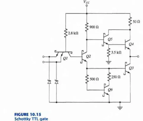
Sch ottky TTL Gate
As me ntionedbefore ,areduction instoragetime results inaredu::Iioa.inPop8Iaf'iondelay.
This isbecau sethe timeneededfor a trans istorto come OUIofsaIUtlItioDdelaysIheswitching
490 Chapter 10 Digit al Integrate d Circuits
ofthe transistorfromthe onconditiontothe off condition.Saturati oncan be eliminated by plac- ingaSchottk ydiodebetween thebase andcollectorofeach saturatedtransistor inthe circuit.
TheSchottkydiodeisformed bythejunctionof ametal andsemiconductor,incontrast to a con- ventional diode,whichisformedbythejunctionofp-type andn-typesemicond uctor material.
Thevoltage acro ss aconductingSchottky diodeisonly 0.4 V.compared with 0.7V ina con- ventionaldiode.Thepresence ofaSchottky diodebetweenthe baseandcollectorpreventsthe transistorfromgoingintosaturation.The resultingtransistoris calledaSchotrkytransistor. The use ofSchottky transistorsinaTILdecreasesthe propagationdelay without sacrifici ngpower dissipation.
The Schottky TTLgate is shown in Fig. 10.15.Note the special symbolused forthe Schottk ytransistorsand diodes.Thediagram shows all transistorsexceptQ-ltobeof the Schottk y type.An exception ismade forQ4,sinceitdoesnotsatu rate. but staysin the acti ve region.Notealso that resistor valueshavebeen reduced inorde rto decreasethe propagation dela yfurther.
Inaddition tousing Schottkytransistorsand lower resistor values,thecircuitofFig.10.15in- cludesother modificationsnotavailable in thesta ndardgateofFig.10.14.Twonewtransistors.
Q5andQ6,havebeenadded, andSchottkydiodesare inserted between each input terminal and ground.Thereisno diode inthe totem-polecircuit.However.thenewcombination ofQ5 andQ4 stillgivesthe twoVBEdropsnecessaryto preventQ4 from conducting when the outputis low.
This combinationconstitutesa doubleemitter-follower called aDarlingtonpair.TheDarlington
so o
9000 2.8kfl:
~Q5 r-
Q''"
r
Q1O J
-~3.5en f-o
QJ
5000 2500
~ ...L
FIGURE10.15 Schottky TIL gate
Section 10.5 Tra nsistor-Transistor logic 49 1
pairprovidesaveryhigh current gain andextremely lowresistance,exactly what isneededduro ing the low-to-high swingof the output,resulting in a decreasein propa gationdelay.
The diodesin each input shown in thecircuithelpclamp any ringin gthatmay occurin the inputlines. Under transien tswitchingconditions,signal linesappear inductive ;this,along with stray capacitance,causes signalsto oscillate,or "ring." Whenthe outp utof a gate switches from thehigh to the lowstate, the ringi ngwaveformat theinputmayhave excurs ionsasgreat as 2-3 V belowground, depending ontheline length .The diodes connec ted to ground help clamp this ringing,since theyconduc tas soonasthenegati ve voltageexceeds0.4V.Whenthe negativeexcursionislimited, thepositive swing is also reduced. Clamp diodeshavebeen so succes sful in limiting line effects that allversionsofTTLgates usethem.
The emitter resistorQ2in Fig. lO.14 hasbeenreplaced in Fig. lO.15bya circuitconsisting of transistorQ6and two resistors. Theeffect ofthis circuit isto reducethe turn off current spikesdiscussedpreviously.The analys isof sucha circuit,whose operation help sto reducethe propagation time ofthe gate, istooinvol vedtopresent inthis brief discu ssio n.
Three-State Gate
As mentioned earlier,theoutputsoftwoTl'Lgates withtotem-polestru ctures cannotbe con- nected together as in open-collector outputs.There is,however,aspecial type of totem-pole gate that allows the wiredconnectio nof outputs forthepurpose of forminga commo n-bussystem.
When a totem-poleoutputTTLgatehasthisproperty,itis calledathree-staregate.
A three-sta tegate exhibits three outputstates: (1)a low-leve lstate when thelower transis- tor inthetotempoleis on andtheuppertransis torisoff, (2)ahigh-level statewhen the upper transistorin the totempole ison andthelower transistor isoff,and(3) athirdstate when both transistors in the totempoleare off.Thethirdstate is anopen-circ uit,or high-impedance, state that allowsa directwire connec tionofmany outp utsto a commonline.Three-stategate s elim- inatethe need foropen-collectorgatesinbusconfigurations.
Figure lO. 16(a) shows the graphicsymbolof athre e-state buffergate.When the control inputC ishigh,thegate is enabled and behaves likea normal buffer,with the output equalto the input binary value.Whenthe controlinputis low, theoutputis anopen circuit, whichgives a high impedance(the third state) regardless of thevalue of inputA.Some three-state gates pro- ducea high-im pedancestate whe n the control inputis high.This is shownsymbolicallyin Fig. 1O.l6(b),where we havetwo smallcircles,onefor the inverteroutputand the otherto indicatethat the gate is enabledwhenC is low.
The circuitdiagram ofthethree-state inverter is shown inFig. IO.I6(c ).Transistors
06.
Q7,andQ8associated withthe controlinputform a circuitsimilar10theopeo-collectorgate. TransistorsQ1- Q5.associated with thedatainpu t, form atote m-poleTI1..circuiLThetwo circuits are connected togetherthrou ghdiode D1.As inanopeo<oUc:c:cor-circuit.transistor Q8turnsoffwhenthe control input atCis inthe low-levelstate.1biIprnaltSdiodeDIfrom conducting. In addition.the emitter inQ1connectedtoQ8basDOcft'dunionpath.Underthis condition, transistorQ8has no effect onthe operationofthe
gare
andtheoutpulillYdepends onlyonthe datainputatA.When the control input ishigh. transistor
Q8
turnson andtheCUItt:DIflowingfrom Vee through diodeD1causes transistorQ8to satura te.ThevoltageIllbcbase01 05isnow
equal492 Chapter 10
Digit al Int egra ted
CircuitsY=Aif C"'high A
---{>---
Yhighimpeda nce~ ifC- low C
(a)Three-stalebuffer gate
Y"'A ·if C=lo....
A
~
Y high impedance ifC=high C(b)Three-state invertergalt'
Co ntrol input C Data input A
10,
I,;I-..:
Q'I Qf\
fQ]
I,; f"Q.l
"'-
Df
...L
-
Q6 f"Q 7
"08
h."
1.':
-J,.
, .
(e)Circuitdiagram forthethree-sta leInverterof (h) FI(i,URE10.16
Three-st ate TTLgate
10.6
Section 10.6 Emitter-Coup led Logic 493
to the voltage acrossthe saturated transistor.Q8.plus one diode drop.or 0.9 V.This voltage turnsoffQ5and Q4.since it islessthan twoVBEdrops.Atthesame time.thelowinput to one oftheemittersof Ql forces trans istor Q3 (and Q2)totum off.Thus.both Q3 andQ4 inthe totempoleareturnedoff. andthe output of thecirc uit behaveslikeanopen circuitwith a very highoutput impedance .
A three -statebusis created by wiring several three-stateoutputstogether.At any giventime, onlyone control input isenabled whileallother outpu tsare in thehigh-impedancestate.The singlegate not in a high-impedancestatecantransmitbinaryinformationthrough thecommon bus. Extremecare mustbetaken thatall except one of the outputsbein the third state; other- wise ,we have the undesirableconditionofhavi ngtwo active totem-pole outputsconnected together.
Animpo rtant featureof most three-stategatesisthatthe outputenabledelay islonger than theoutput disabledelay.If acontrol circuitenablesonegateand disablesanotherat thesame time.thedisabledgateentersthehigh-impedancestate beforethe othergateisenabled. This eliminatesthe situation of both gatesbeingactive at the sametime.
There isa verysmall leakage current associated with the high-impedance conditio nin a three-state gate. Nevertheless.thiscurrent isso smallthat as many as 100three-state outputs can beconnected togetherto form a common-busline.
EMITTER -COUPLED LOGIC
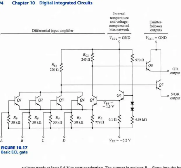
Emitter-coupledlogic(ECL) is anonsaturateddigital logic family.Sincetransistorsdo notset- urate. itispossible toachievepropagationdelays aslow as 1-2ns.Thislogic familyhasthe lowest propagationdelayof any familyand isused mostlyinsystems requiringvery highspee d operation.Itsnoise immunity and power dissipation.however.are the worstof allthelogic fam- ilies available.
A typicalbasiccircuit of theEeLfam ilyisshown in Fig. 10.17.Theoutp utsprovideboth the OR and NO Rfunctions.Eachinputisconnected tothe base of a transistor.The two volt- age levels are about- 0.8 V for the high state andabo ut- 1.8 V for the lo w state.Thecircuit consistsofa differentialamplifier. a temperature-andvoltage-compe nsatedbiasnet work.and an emitter-followeroutput. The emitteroutputsrequire a pull-down resistor forcurrent toflow.
Thisisobtai nedfromtheinputresistorRpof anothersimilargateorfromanextern alresistor connectedto a negativevoltagesupply.
The internaltempe rature-and voltage-compensated bias circuitsuppliesa reference volt - age to thedifferentialamplifier.Biasvoltage Vssissetat - 1.3 V, whichis
me
midpointofme
signal'slogicswing.Thediodesinthevoltage divider.fogetberwithQ6.providea circuit that maintainsa constantVBsvalue despitechangesintemperature or supplyvoltage.Any one of the power supp lyinputs could beusedasground.However,the useoftheVccnodeas ground andVEEat- 5.2 V resultsinthebestnoiseimmunity.
If any inputinthe ECLgate ishigh.the correspondingtransistor istumedOIl and Q5is turnedoff.An input of- 0.8 V causesthe transistorlOconduetandplaces -1.6VOIltheemit- tersofall of thetransistors. (The VB£drop inEeLtransistorsis0.8 V.)SinceVB B = - 1.3V, the base voltage ofQ5isonly0.3Vmore positive
man
itsemittet.Q5is cutoffbecauseitsVBE494 Chapter 10 Digital Integra ted Circuits
Differential inputamplifier
Internal temperature andvoltage- compensated
biasnetwork
Emitter- follo....er OUtputs
:-';OR output OR output Veel - O:-iD
i
Vee: . GND
r e+-
Rn
2450 970n
v.:
R" ~Q8
2200
I
Q7
<16 1--
1~l ~2 ~3 ~4 Q'j-1 ,A
-V,II1.3VB=,
r-r- r-t- r-t- r-r-
R, R, R, R, R,
6.1
n
4.98knso e n
SOlO SOkH 50kO 779 nA B
c
D VEE"" -S.2VFIGURE10.17 Basic ECl gate
vol tageneeds atleast0.6V tostanconducting.ThecurrentinresistorRc:flowsintothe base of Q8 (provided thatthereisa loadresistor).This currentis so smallthatonly a negligible voltagedrop occurs acrossRcz-TheORoutputofthegate is oneVBEdropbelow ground.or - 0.8V.whichisthe high stale.The current flowingthroughRCI andthe conductingtransis- torcausesadropof about1V belowground.(SeeProblem10.9.)The l'\ORoutput isoneVBE dropbelowthislevel. or - 1.8 V.whichisthelow stale.
Ifall inputsare atthelowlevel,allinput transistors tumoff andQ5conducts.The voltage in the commo n-emitternode isoneVBEdrop belowVBB,or- 2.1V.Sincethebase of eachinput isatalowlevel of- 1.8 V.eachbase-emitterjunctionhas only0.3V andallinputtransistors are cut off.RCl draws current throughQ5that resultsinavoltagedrop ofabout IV,making theORoutputoneVBEdrop below this.at-1.8V.orthe lowlevel.The current inRClisneg- ligible.andtheNOROUtpUIis oneVBEdrop belowground, at - 0.8V.orthe high level.This analysisverifiesthe ORandNORoperatio nsof thecircuit.
The propagation delayoftheEe Lgaleis2nsand the powerdissipationis25mw,giving a speed-power prod uct of50.whic hisaboutthesame asthat for theSchottkyTIL. The noi se
Section 10.7 Metal-Oxide Semiconductor 495
(A +B)' ... (C+DJ'=
[(A +BltC+D)I'
+i4-- - -
(AT B)(C+D)A
B-L:...~-.
c- G*- -+_ ...J
D
A-~,;",_(A..,.ByNOR
B (A+B) OR
(a) Singlegate (b)Wired combination oftwo gates
fiGURE 10.18
Graphic symbolandwiredcombi natio nofECL gates
margin is about 0.3Vand isnotasgood asthat in theTTLgate.Highfan-out ispossible in the EClgate because ofthe highinputimpedance of thedifferential amplifierand the low output impedan ceofthe emitter-follower. Because of theextreme high spee dofthesignals.
external wires act liketransmission lines. Except for verysha lt wiresof a few centimeters.
ECl outputs must usecoaxia lcables witharesistor terminationtoreducelinereflections.
The graphicsymbol for theEClgate shown inFig. 10.18(a).'TWo outputsare available:one fortheNO Rfunction and theother forthe ORfunction.The outputsoftwo ormoreECL gates can be connec ted togetherto formwired logic.As shownin Fig.1O.18(b ),anexternalwired connectionof twoNORoutputsproducesawired-ORfunction.Aninternalwired connection of two ORoutp utsisemployed insome EelICstoproduce a wired-AND(sometimescalled dot- AN D) logic . This property may be utilized when ECL gales are used to form the OR-AND-INVE RTand theOR-ANDfunctions.
10 .7 METAL -OXIDE SEMICONDUCTOR
The field-effect transistor(FET) is a unipo lartransistor.since its operation dependsonthe flow of onlyonetype of carrier.Thereare twotypesofFETs:the junctionfield-effecttransis- tor (JPET)and the metal-oxidesemiconductor(MaS).Thefanner isused in linear circuits and thelatter in digitalcircuits. MaS transistors can befabricated in lessarea than bipolar transistors.
Thebasic structureofthe MOS transistoris shown in Fig .10.19.1bep-channelMOS con- sists of a lightlydoped substrate ofa-typesilicon material.Two regions are heavilydopedby diffusionwithp-typeimpuritiestofonnthe sourceanddrain.1beregionbetweenthetwo~
typesectionsservesasthechannel.Thegaleisametal plate separatedfromthedwmeIbyan insulated dielectri c ofsilicondioxide.Anegativevoltage(withrespecttotbesubsuaIe)81the gate terminalcausesaninduced electricfield inthechanne lthatattraetsp-eype carriers(ho&es) from thesubstrate.Asthe magnitude of thenegati vevoltageonthepte iD:reases, theregion below the gale accumulates morepositivecarriers.theoonduaivity
increases.
andC\lI'ttnlcan nowfromsource to drain.providedthat a voltage differenceismainlaioed betweenthesetwo terminals.496 Chapter 10 Di gital Int egrated Circuits
{alp-cha nnel FIGURE 10.19
Basic st ruct ureofMOStransisto r
(b) u-channe l
Thereare fourba-le typesof~fOS structures.Thechannelcan bepor11 type.depending onwhether the majoritycarriers are holesor electrons.The modeof operationcanbe en- hancementordepletion. dependin g on the state of thechannelregionatzero gate voltage.If thechannel isinitiallydoped lightly with p-typeimpurity(inwhichcaseit isca lledadiffused channels.aconducting channelexistsatzerogatevoltage and thedeviceis saidtooperatein thedeplet ion mode.In this mode. current flowsunlessthe channelisdepletedbyan applied gatefteld.lftheregion benea th thegaleisleflinitiallyuncharged. a channelmust beinduced bythegalefieldbeforecurrentcanflow.Thus.thechannel current is enhanced by the gatevolt- age.andsuch adevic eis said to operatein theenhancement mode.
Thesource isthe termi nalthrough whic hthemajoritycarriers enterthedevice.The drai n isthe terminal throughwhich themajoritycarriersleaveIhedevice.In an-channel MOS.the source term inalis connected tothesubstrate anda negativ evoltage isapplied to thedrain term ina l.Whe n the gale milage isabovea threshold voltage V
r
(abo ut - 2V).no currentflowsinthe channelandthe drain-to-sourcepath islike an opencircu it.When thegatevolt- age issufficientlynegativebelow VT•achannelisformedandp-type carriersflowfrom source
10drai n.p-Iypecarriersarepositi ve andcorrespondto a positivecurrentflowfrom source10 drai n.
In the u-channe! f\.IOS. thesourcetermin al isconnected tothesubstrate anda positive\011· age is applied tothe drainterminal.Whenthegale voltageisbelowthe thre..holdvoltage V
r
(about 2 V).nocurrent flows in the channel. When thegate voltage issufficiently positive above Vr to fonn the channel,a-typecarriers flo... from source 10 drain.n-typecarriersare negative andcorrespondtoa positive current flow from draintosource.Thethresholdvoltage may vary from I104V,depending ontheparticularprocessused.
Thegraphicsymbolsfor theMOStransistors areshown inFig.10.20.Thesymbol forthe enhancementtypeistheone withthebroken-line connec tionbetwee nsourceanddrain.Inthis symbol.the substratecan be identifiedandis shownconnectedtothesource.Analternative sym- bol omitsthesubstrate.and insteadanarro... is placedin the sourcetermin al10 showthe di- rection of
positive
currentflow(fromsource todrainin the p-channel MOSandfrom drainto sourceinthe II-channel MOS).Because ofthesymmetricalconstructionofsource and drain.the tl.l0S transistorcanbe operatedasa bilateraldevice.Although normally opera tedsothatcarriers flowfrom sourceto drain.there arecircumstances when ir isconvenient 10 allow carriers to flow from drain to source.(SeeProblem10.12.)
Section 10.7 Metal-Oxide Semiconductor 497
drain
~alC
--1 q .-J
sub!.trateW"=
D
G -< s
drain
~ate
--1 .-J 1---
sub!.lralc'I
sourceD
G - <
s
(a) p-channe l fiGURE 10.20
Sym bo ls for MOS transistors
(b)e-channel
Oneadvantage oftheMOS deviceisthatitcanbeusednOIonlyasatransistor,butas are- sistoras well.Aresistorisobtained from theMOS bypermanently biasingthegatetermin al forconduction. Theratio ofthesource-drain voltagetothechannelcurre nt then determine s the valueof theresistance.Different resistor value smayheconstructedduring manufacturingby tixingthechannellengthand width of theMOS device.
Three logic circuitsusing MOSdevices are shown in Fig. 10.21. For ana-channel MOS, the supplyvoltage Vnn is positive (about 5V).toallow positi vecurrent flow from drain to source.TheIWOvoltagelevelsareafunction ofthe threshold voltageVr.The lowlevel isany- where fromzerotoVr•andthehighlevel rangesfromVTttlVnn.Then-channelgates usually employ positivelogic.Thep-channel~10Scircuit..U~a negative voltageforVnl).10allowpus- itivecurrent flowfromsource 10 drain.TheIWOvoltage levelsare both negativeaboveand below thenegativethreshold voltageVr.n-channelgalesusuallyemploynegati velogic.
r - - " - ----r--
Y- (Ao +BfY= (A B)'
\' OD
I
y- A'
[ajInverter (b)SAN Dp iC (c)NOR11*
FIGURE 10.21
n-<h annel MOS logic circuits
498 Chapter 10 Digital Integrated Circuits
The invertercircuitshown in Fig.1O.21(a)uses two MOS device s.QJactsastheloadreo sistorandQ2as theactive device.The load-resistorMOS has its gate connectedtoVDD•thus maintaining it inthe conductionstale. When the inputvoltageislow(belowVr).Q2turnsoff.
SinceQJis always on. the outputvoltage is aboutVDD.When the input voltage ishigh(above Vr).Q2tum s on.Current flowsfromVDDthrough theload resistorQJand intoQ2.Thegeom- etryofthe two MOS devicesmustbesuch that the resistance ofQ2.when conducting .ismuch lessthan the resistance ofQJto maintaintheoutputYat a voltagebelowVr.
TheNAl\'D gateshownin Fig.10.21(b)usestransistors inseries.InputsAandBmust both be high for alltransistorstoconduct and causetheoutputtogo low.If eitherinputislow.the corresponding transistoristurnedoff andtheoutputishigh.Again.the seriesresistanceformed bythe two activeMOS devicesmust bemuch less than the resistanceoftheload-resistor~10S.
The NORgateshown inFig.1O.2H c)usestransistors inparallel.If either inputis high.the cor- respondingtransistorconducts andtheoutputislow.Ifall inputs are low,allactive transistors are off and the outputishigh.
10 . 8 COM PLEM ENTARY MOS
Complementary MOS (CMOS) circuit stake adva ntageofthe factthai both n-channe l and p-channel devicescanbefabricated on thesamesubstrate.CMOScircuitsconsist ofbothtypes of MOS devices.interconnectedto formlogic functions.The basic circuitisthe inverter,which consistsofonep-channeltransistorandone n-channel transistor.asshownin Fig. 1O.22(a).
The sourceterminalofthe p-channeldevice is atVDD•and the sourceterminalof the a-channel deviceisatground.The valueofVDDmaybeanywherefrom
+
3 to+
18V.Tbetwo voltage lev- els area v
for the lowlevelandVDDfor the high level(typically.5 V).Tounderstand the operationof theinverter,we must review the behaviorof theMOStran- sistorfromthe previou s section:
1. The a-chan nel MOSconducts when its gate-to-so urcevoltage ispositive.
2. The n-channelMOS conducts when itsgale-to-source voltageisnegative.
3. Either typeofdevice isturned offifits gate-to-source voltage is zero.
Now consider theoperationof the inverter.Whentheinputislow.bothgates are atzeropo- tential.Theinput Isat - VDDrelative to the sourceof thep-channel dev