Additional information is available at the end of the chapter http://dx.doi.org/10.5772/intechopen.78963. In this book, some of the key applications in sensors and waveguides have been highlighted. Additional information is available at the end of the chapter http://dx.doi.org/10.5772/intechopen.76439.
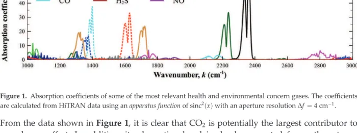
Of the initial works in MPS development, it is also worth mentioning those by Zhang [5], Propst [6] and Parkhutik [7]. In particular, environmental monitoring for pollution control [25, 31] is one of the most important applications. The absorption spectrum of a gas at these light frequencies is caused by the different vibrational and rotational modes of the atomic bonds in the molecules [35].
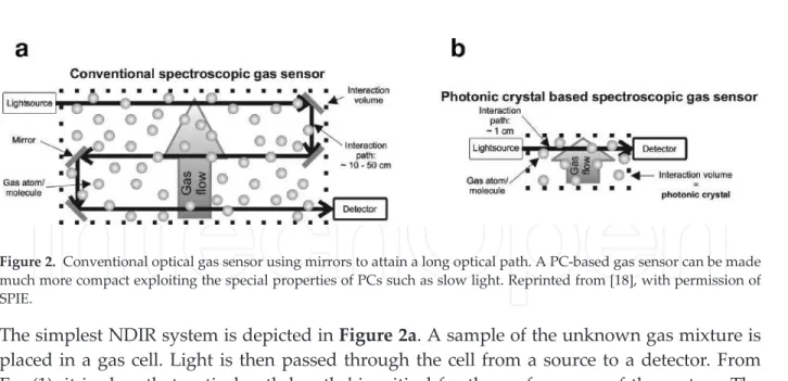
The absorption coefficient spectra of several of the environmental gases are plotted in Figure 1. Identification and quantification of a particular gas can be done by looking at a narrow band region of the spectrum. At the other end, the detector (a photodiode: PD) will provide a measure of the received optical power, directly corresponding to the concentration of the gas.
1), it is clear that the length of the optical path l is critical for the operation of the system.
Macroporous silicon applied to gas detection
One of the first uses of MPS for gas sensing is in the work of Geppert [18]. They show promising results, but they argue that the small numbers obtained are due to the low coupling efficiency of the computer. To avoid this problem, a special tapered section is placed on the interfaces of the computer.
These are attributed to manufacturing uncertainties: a 1% variation in pore diameter is reported. The simplest for low frequencies is to calculate the average of the various materials that make up the computer. The general description of the method is the dissolution of silicon by an electrically accelerated reduction-oxidation chemical process (redox reaction).
Thanks to this behavior, it is possible to use the EE method to fabricate 3-d MPS structures by modulating the current and potential during the etching process [49]. In a minimal sense, macroporous silicon is of "good quality" if pores have the same shape and have grown uniformly. Unstable growth is basically caused by substrate inhomogeneity, although the dynamic behavior of the etching system can also affect [51].
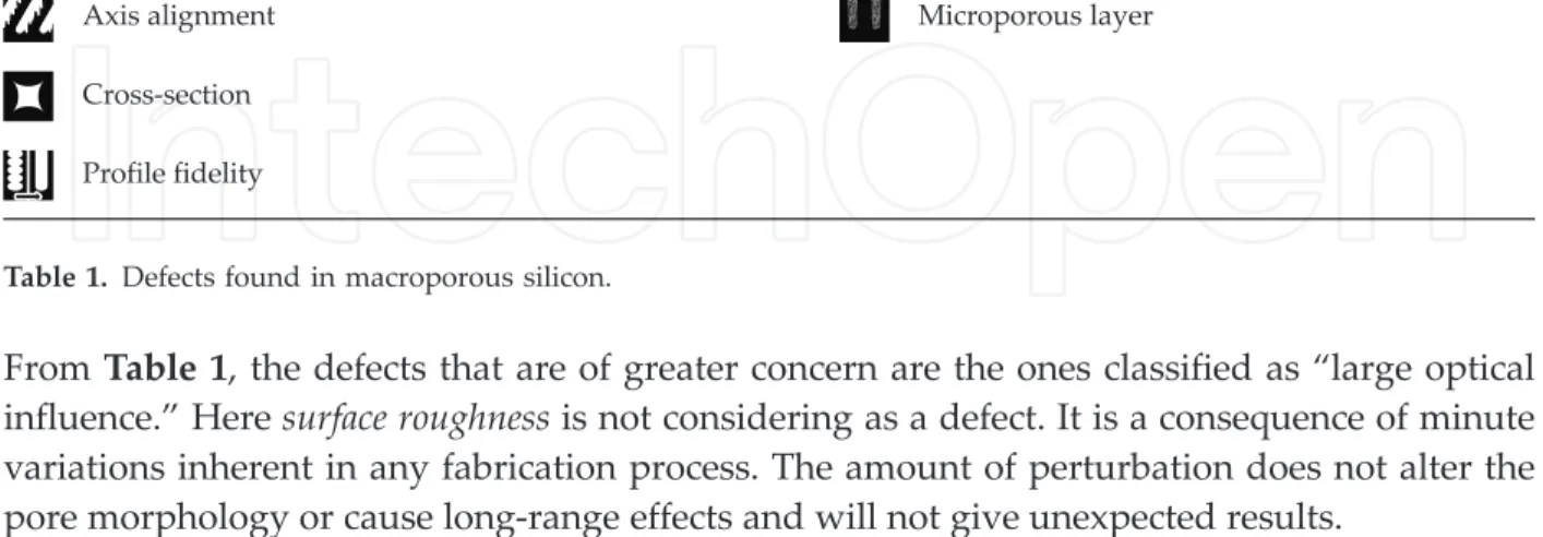
Profile fidelity refers to the closeness of the actual pore profile to the intended profile. The above discussion was made taking into account the local effect of perturbations in the pore shape and the result of the etching process. Nevertheless, the uncertainties of etching, substrate inhomogeneity, and errors in lithography can be considered larger scale or long-range.
An important concern is determining how absorption and manufacturing tolerances will affect the performance of the detection system. For example, it is reported in [17] that a 1% variation of pore radius attenuates 15 dB=cm of the transmitted light. A systematic study of the effect of in-plane perturbations in electrochemically etched MPS is presented in [56].

Measurements and results
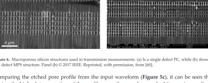
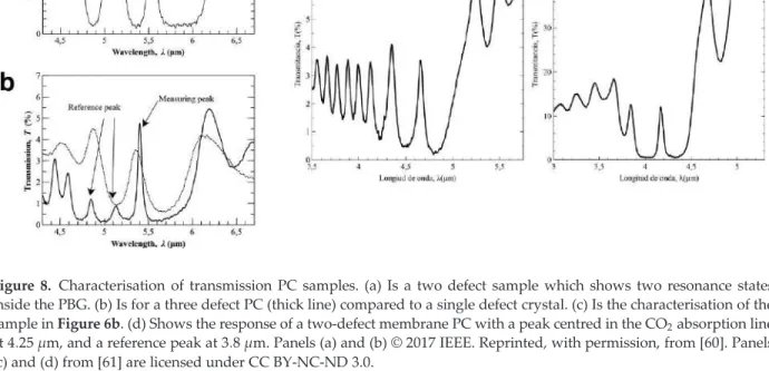
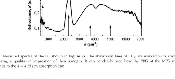
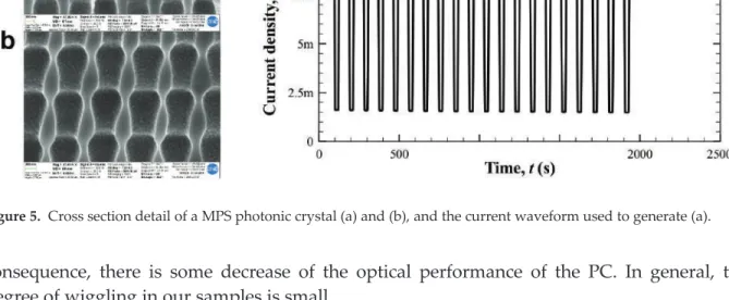
The cross-sectional images show that the modulation is slightly skewed after the start of the modulation. This significantly improves the PBG (both width and transmission blocking) of the PC compared to the first structures depicted in Figure 5. The vertical period of the PC used for these samples is pv≈1μm. It can be clearly seen how the PBG of the MPS structure corresponds to the λ¼4:25μm absorption line.
Coupling between resonant cavities induces the appearance of multiple resonances in the optical spectra, even though all cavities are of the same dimensions. The location of the defect along the PC depth also affects the resonant coupling efficiency and quality factor. The creation of a membrane also improves the transmitted signal, compare Figure 8, where the transmitted peak is almost 10% to 4% of the non-membrane sample.
The expected response of an autonomous NDIR measurement device can then be extrapolated from the collected spectroscopic data to characterize the PCs. The basic idea proposed here for an NDIR system is to use an MPS photonic crystal with a PBG wide enough to include one of the gas absorption regions. In the following discussion, it is assumed that the DP response is flat in the gas absorption region.
From the characterization measurements, it is easy to approximate the expected response of the NDIR system. Spectra can be either reflection, transmission, or absorption, since these are proportional to the power of the electromagnetic wave: jErð Þλ j2 ¼ Rð Þλ jEið Þλ j2, and so on. The relation of this quantity to an actual output of a PD is less clear, but it serves to evaluate the performance of the gas cell and the PC.
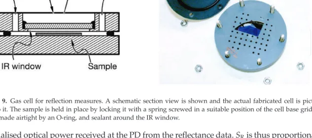
The use of a reference spectrum removes any effects of the optical system, such as reflection at optical interfaces. The sample is held in place by locking it with a spring screwed into a suitable position of the grid of the cell base. For example, the thickness of the MPS sample or the tightening of the screws can change the gap by up to 0:2 mm.
Conclusion
This effect is then observed in the "optical effect" signal Sat output (Figure 10b) calculated as mentioned above. Using silicon as a base material has other advantages, such as reuse of the existing production tooling and reuse of process streams. It has been shown that the MPS crystal also has an effect in the measured absorption.
This is due to the nature of the PC, which slows the group velocity of the incident light and improves the interaction time - increasing the effective optical path length - with the gas mixture. The authors would also like to thank the contribution and assistance of Daniel Segura García and David Cardador Maza in the preparation of this chapter. The effect of absorption losses on the optical behavior of macroporous silicon photonic crystal selective filters.
Macroporous Silicon: Homogeneity Investigations and Fabrication Tolerances of a Simple Cubic Three-Dimensional Photonic Crystal. Selection of our books indexed in the Book Citation Index in Web of Science™ Core Collection (BKCI).
TOP 1%
New Approach to Mach-Zehnder Interferometer (MZI) Cell Based on Silicon Waveguides for Nanophotonic
- Introduction
- MZI cell based on directional couplers
- MZI cell based on 2 2 multimode interference coupler
- MZI cell based on a 4 4 MMI coupler
- Waveguide mesh design with new MZI cell
- Conclusions
In [22], the author has presented a universal self-guided beam coupler based on MZI elements that can take an arbitrary monochromatic input beam and, automatically and without any calculations, combine it into a single-mode guide or beam. Using the recursive algorithm, any discrete finite-dimensional unitary operator based on MZI elements can also be constructed [23]. Furthermore, it was shown that optical neural networks based on the architecture of 56 MZI with 213 thermo-optical phase shift elements have been successfully implemented [24].
Consequently, it is attractive to realize new functional devices based on MMI for photonic applications. In this chapter, we present a new MZI element architecture based on only one 4 4 MMI coupler on the SOI platform. A PN junction based phase shifter using plasma. dispersion effect in silicon waveguides.
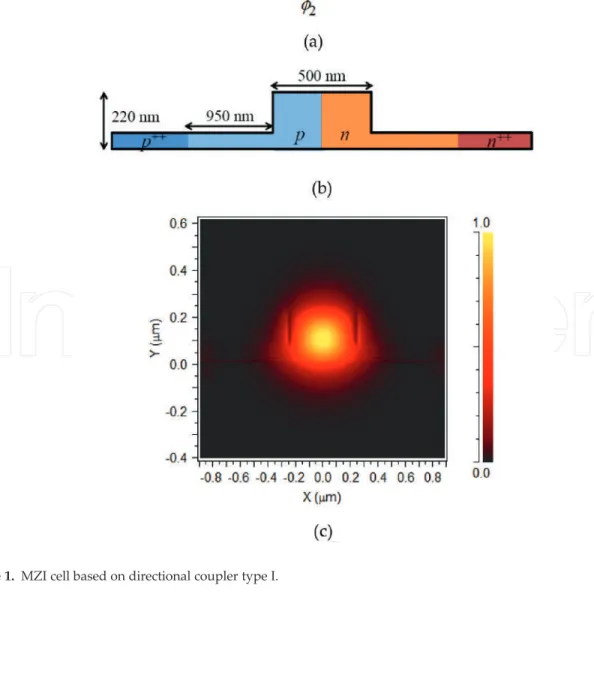
An MZI cell based on a directional coupler of type I. and the real part of the phase can be significantly increased compared to the bias. The ratio matrix between the input and output fields of the MZI can be expressed as [30]. From these simulation results, we can obtain the optimal length of the directional coupler for a 50:50 coupling ratio or a 3 dB coupler. Figure 2(c) shows the field spread for a 3 dB coupler with g = 120 nm and an optimal length of 5 μm.
From these simulation results, we can arrive at the optimal directional coupler length for 50:50 coupling ratio or 3 dB pair. Figure 4(c) shows a field spread for a 3 dB coupler with g = 120 nm and optimal length of 2μm. . The operation of an MMI coupler is based on the principle of self-imaging or the Talbot effect [31, 32]. There are two ways to create a 3 dB coupler based on the MMI principle [20]: the first is the general interference (GI) mechanism which is independent of the modal excitation (we call it type I MMI coupler in this chapter).
The normalized outputs of the 22 GI-MMI links at different link lengths are plotted in Figure 8. The normalized outputs of the 22 RI-MMI links at different link lengths are plotted in Figure 10(a). By some calculations, the MZI cell based on 4 4 MMI coupling can be expressed by a characterized matrix.
Microring resonator based on 3 3 general multimode interference structures using silicon waveguides for highly sensitive sensing and optical communication applications. Design of optical signal transformations based on planar waveguides on a silicon-on-insulator platform.