GATE LEAKAGE IN LOW STANDBY POWER OF 18nm GATE LENGTH MOSFET
NOORFARIDAH BT ABDULLAH@YAACOB
This Report Is Submitted In Partial Fulfillment Of Requirements For Bachelor Degree Of Electronic Engineering (Computer)
Fakulti Kejuruteraan Elektronik Dan Kejuruteraan Komputer Universiti Teknikal Malaysia Melaka
v
DEDICATION
vi
ACKNOWLEDGEMENT
“In the name of Allah, the most Gracious, most Powerful, and the most Merciful”
Firstly, praise to Allah SWT for guiding and blessing with perseverance and strength to complete the project. Without the strength gave to me from the God, this project report cannot be finish within the time provided. First of all, I would like to express my biggest appreciation to my beloved Project Supervisor , Dr Anis Suhaila Bt Mohd Zain for all her precious supports and advises during completing this project report. Furthermore, she guides me consistently and gives full dedication throughout the semester.
I also would like to thank my beloved parents especially my father and my mother for giving me the truly support and motivation to finish this project report. I am very appreciating of their understanding towards my commitment to finish the PSM report. Bundle of thanks to my friends especially to those who gave me the precious help and support in completing this project. Last but not least, I would like to thanks all the people who have involve directly and indirectly to give contribution due to complete the PSM.
vii
ABSTRACT
viii
ABSTRAK
ix
TABLE OF CONTENTS
CHAPTER TITLE PAGES
PROJEXT TITLE i
DECLARATION ii
DEDICATION iii
ACKNOWLEDGEMENT vi
ABSRACT vii
ABSTRAK viii
CONTENTS ix
LIST OF TABLES xiii
LIST OF FIGURES xiv
I INTRODUCTION 1.1 INTRODUCTION OF PROJECT 1
x
1.3 SCOPE 3
1.4 PROBLEM STATEMENT 4
1.5 PROJECT OUTLINE 4
II LITERATURE REVIEW
2.1 INTRODUCTION 6
2.2 LEAKAGE CURRENT 8
2.3 THRESHOLD VOLTAGE VS GATE LENGTH 9
2.4 DIELECTRIC MATERIALS 11
III METHODOLOGY
3.1 PROJECT METHODOLOGY 15
3.2 DESIGN OF MOSFET STRUCTURE 18
3.2.1 Step by Step on Process Simulation 18
xi
IV RESULT AND RECOMMENDATION
4.1 INTRODUCTION 30
4.2 PROJECT DESIGN 31
4.2.1 Polysilicon with 18nm gate length (Lg) 31
4.2.2 Polysilicon with 20nm gate length (Lg) 33
4.2.3 Polysilicon with 30nm gate length (Lg) 35
4.2.4 Titanium with 18nm gate length (Lg) 37
4.2.5 Titanium with 20nm gate length (Lg) 39
4.2.6 Titanium with 30nm gate length (Lg) 41
4.3 OVERALL PARAMETERS FOR STANDARD
STRUCTURE MOSFET (ITRS 2011) 43
4.4 GRAPH LINEAR AND CURVES LOG ID………..
AGAINST VGS FOR STRUCTURE USING...
xii
V CONCLUSION AND RECOMMENDATION
5.1 CONCLUSION 59
5.2 RECOMMENDATION 60
VI REFERENCES 61
xiii
LIST OF TABLE
NO TITLE PAGE
1.1 Example of materials with its dielectric constants. 2
2.1 Threshold voltage for three cases of gate length 11
2.2 Dielectric constant (k) and its conduction band 12
3.1 Low standby power technology requirement of ITRS 16
4.1: Parameter scale of 18nm gate length (Polysilicon) 16
4.2: Parameter scale of 20nm gate length (Polysilicon) 32
4.3: Parameter scale of 30nm gate length (Polysilicon) 34
4.4: Parameter scale of 18nm gate length (Titanium Nitrate) 36
4.5 : Parameter scale of 20nm gate length ( Titanium Nitrate) 40
4.6: Parameter scale of 30nm gate length (Titanium Nitrate) 42
4.7 : Overall Parameters for Standard Structure MOSFET (ITRS 2011) 43
xiv
LIST OF FIGURE
NO TITLE PAGE
2.1 Structure of MOSFET [2] and the NPN transistor based
on nMOSFET 7
2.2 Ilustration of gate direct tunneling component 8
2.3 Tunneling of gate leakage 8
2.4 Graph for drain current versus Drain-Source voltage with 500 nm …
transistor lengths (small gate length) 9
2.5 Graph for drain current versus Drain-Source voltage with 500 nm….
transistor lengths (moderate gate length) 10
2.6 Graph for drain current versus Drain-Source voltage with 500 nm…
transistor lengths (large gate length) 10
2.7 High k material 13
2.8 Improvement of F-N tunnel current densities with high-k gate …….
dielectric 14
2.9 Improvement of direct tunnel current densities with gate voltage for..
xv
3.17 Adjusted aluminium position 26
3.18 Full structure 26
3.19 Electrode on gate 27
3.20 Electrode on source 27
xvi
3.22 Flow of Atlas in order to get the result 29
4.1 (a) MOSFET design of 18nm gate length 31
4.1(b) Contour structure after doping 32
4.2 (a) MOSFET design of 20nm gate length 33
4.2 (b) Contour structure after doping 34
4.3 (a) MOSFET design of 30nm gate length 35
4.3 (b) Contour structure after doping 36
4.4 (a) MOSFET design of 18nm gate length 37
4.4 (b) Contour structure after doping 38
4.5 (a) MOSFET design of 20nm gate length 39
4.5 (b) Contour structure after doping 40
4.6 (a) MOSFET design of 30nm gate length 41
4.6 (b) Contour structure after doping 42
xvii
4.17 Graph linear and Curves Log ID against VGS for 20nm in 1V 54
1
CHAPTER 1
INTRODUCTION
Chapter 1 covers about the introduction part of this Final Year Project of Degree. It contains subchapter of objectives, problem statements, scopes of projects and project outline.
1.1 Introduction of Project
2
In MOSFET structure, it has 4 terminals; source (S), gate (G), drain (D), and body (B). In semiconductor, there are three categories according to performance, which are high performance, low standby power, and low operating power. Leakage current happens to all categories which are a gradual loss of energy for charging capacitor. It may reduce the performance of electronic product. Leakage current of MOSFET consists of three components called off-state sub threshold leakage current, gate direct tunneling leakage current and source/drain junction leakage current.
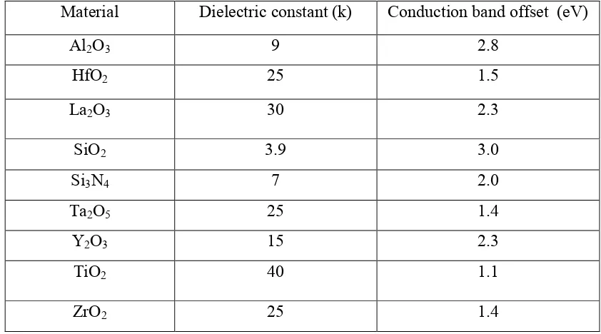
By adding high dielectric constant (k) oxides, it will reduce the leakage current and improve the performance of the MOSFET. High dielectric constant (k) oxides have some requirements which are good insulating properties, good thermal stability, capacitance performance, and high crystallization temperature. Table 1 shows several materials with its dielectric constant (k).
Table 1.1: Materials with different dielectric constants.
Material Dielectric constant (k) Conduction band offset (eV)
3
1.2 Objective
The objectives of this project are:
1. To design 18nm, 20nm and 30nm of gate length N-MOSFET in Low Standby
Power.
2. To investigate the impact of different gate oxide materials on threshold voltage and drive current for similar materials with different gate length. 3. To investigate the impact of different gate oxide materials on threshold
voltage and drive current for similar gate length with different material.
1.3 Scope
4
1.4 Problem Statement
Previously, MOSFET structures use silicon dioxide (SiO2) to avoid gate leakage. However, for a long time, the thickness of silicon dioxide (SiO2) reduced accordingly. This will reduce the performance of silicon dioxide (SiO2) and leakage current will increase in order to supply current from source to drain.
In addition, theoretically shorter gate length, will provide high density of current from drain to source. Thus, reducing of gate length from previous design is 30nm to 20nm and to 18nm was being designed. However, these changes will cause some disruption electrostatic force on the MOSFET. To handle these weaknesses, the best two materials were chosen to add on silicon dioxide (SiO2) in order to keep the performance.
1.5 Project Outline
The outline of this project is planning to ensure the flow of this research study is done properly. Besides that, this outline also can help the readers to fully understand the objective and the content of this thesis.
The report consists of five chapters which is Chapter 1 will discuss about the introduction of the project, which includes the objectives of the project, problem statements, scope of the project, and project outlines. The problem statement describes the problem faced by the performance of each topology and followed the discussion of the scope and significance of the project.
5
Chapter 3 explaining the project flow from the starting until the end. In this chapter a briefly explain the procedures to design the MOSFET. It consists of the theoretical for the Silvaco software simulation including DEVBUILD and ATLAS.
Chapter 4 is the discussion stage where the result and the finding are presented. It consists of the explanation for the data and the problem occurred since the research begins and the update design to improve the finding result. Analysis from transfer curves and sub threshold curves also discussed in this chapter.
6
CHAPTER 2
LITERATURE REVIEW
This chapter presents an overview of the previous works on the related topic for the background study.
2.1 Introduction
7
According to the performance of semiconductor devices, ITRS classify them into three categories which are high performance, low standby power, and low operating power. Low operating power was used for low performance device and low cost consumer type application [8] [15]. Low standby power is usually used for low power consumption, actually to preserve battery life. Thus, the best solution to reduce the power dissipation is lowering the power supply voltage (VDD) [1].
![Figure 2.1: Structure of MOSFET [2] and the NPN transistor based on nMOSFET](https://thumb-ap.123doks.com/thumbv2/123dok/496656.55392/24.595.207.431.269.617/figure-structure-mosfet-npn-transistor-based-nmosfet.webp)
