DESIGN AND CHARACTERIZATION OF 20NM SOI MOSFET DOPING ABRUPTNESS DEPENDENT
NOR FATIHAH BINTI MOHD ZAIN
This report is submitted in partial fulfillment of requirement for the award of the Bachelor Degree of Electronic Engineering (Computer Engineering)
Faculty of Electronic and Computer Engineering Universiti Teknikal Malaysia Melaka
v
ACKNOWLEDGEMENT
Alhamdulillah, I would like to extend my deep gratitude toward the almighty Allah S.W.T because give me the strength, idea and patience to complete my Final Year Project (PSM).Without your permission, I was not able to continue this project sucessfully.
My sincere appreciation for my Final Year Project supervisor, Dr. Anis Suhaila binti Mohd Zain because give me a chance to work under her supervision. You are the one who most help me by give me a lot of ideas, very useful knowledge, encouragement and full support in all guidance. Thank you for willing to spend a lot of time for me and giving your patience in completing this project. I will always remember your kindness until until the end of my life.
Special thanks I also would like to express to my beloved parent, Mohd Zain bin Dollah and Zukiriah binti Mat Zin for their love and support me all the time through my life. The one who give me strenght to continuing my studies and always pray for my success. Thanks also for my lovely sibling that always concern and give lot of motivation to me. I will do my best for the sake of our family.
Also, i does not forget to say a lot of thanks to my friend and my colleagues especially Nurezzaty binti Jamaluddin, Noorfaridah binti Hj Abdullah @ yaacob and Nela Putri Warni binti Azizi. Thank you for working together with me and always give me idea and support to complete this project. Your laugh able to reliase my stress during process of completing this final year project.
vi
ABSTRACT
vii
ABSTRAK
viii
TABLE OF CONTENT
CHAPTER TITLE PAGE
PROJECT TITLE i
REPORT STATUS VERIFICATION FORM ii
ix
1.5 REPORT STRUCTURE 3
II LITERATURE REVIEW
2.1 Introduction 5
2.2 Field-Effect Transistor (FET) 5 2.3 What is Silicon on Insulator (SOI) 6
2.3.1 Basic Construction 6
2.4 History of Silicon on Insulator 8
2.5 MOSFET Scaling 10
2.6 Limitation of MOSFET Scaling 11
2.7 Doping Abruptness 12
III
PROJECT METHODOLOGY
3.1 Introduction 14
3.2 Methodology 14
3.3 Step of creating the SOI MOSFET using Silvaco
x
SOI MOSFET
4.4.1 3.3 nm/dec Doping Abruptness SOI
MOSFET Device 28
4.4.2 3.5 nm/dec Doping Abruptness SOI
MOSFET Device 33
4.4.3 3.8 nm/dec Doping Abruptness SOI
MOSFET Device 38
4.5 Summary of Doping Abruptness Dependent of
SOI MOSFET 43
V CONCLUSION AND RECOMMENDATION
5.1 Conclusion 46
5.2 Recommendation 47
REFERENCES 49
APPENDIX A 51
APPENDIX B 53
xi
LIST OF TABLES
NO TITLE PAGE
2.1 History of development of SOI technology 10 3.1 The values and dimension of the device parameter [3] 17 4.1 Physical Device Parameter for 20nm device 25 4.2 Electrical Characteristic value of 3.3 nm/dec doping
abruptness with 1V drain voltage 30 4.3 Electrical Characteristic value of of 3.3 nm/dec doping
abruptness with 50mV drain voltage 32 4.4 Electrical Characteristic value of of 3.5 nm/dec doping
abruptness with 1V drain voltage 35 4.5 Electrical Characteristic value of of 3.5 nm/dec doping
abruptness with 50mV drain voltage 37 4.6 Electrical Characteristic value of of 3.8 nm/dec doping
abruptness with 1V drain voltage 40 4.7 Electrical Characteristic value of of 3.8 nm/dec doping
abruptness with 50mV drain voltage 42 4.8 Summary of the electrical characteristics of doping abruptness
xii
LIST OF FIGURES
NO TITLE PAGE
2.1 Comparison of bulk and SOI structure 7
2.2 SIMOX Process 8
2.3 ELTRAN process flow [14] 9
2.4 Numbers of transistor according Moore’s Law [18] 11
2.5 Graph of doping concentration 13
3.1 Flowchart of the process to create the SOI MOSFET 15
3.2 Three main SOI layer [10] 16
3.3 Bulk structure of SOI MOSFET 17
3.4 Oxide was deposit (BOX) 18
3.5 Body part was deposit 18
3.6 Creating of Mask layer 19
3.7 The doping was implanted 19
3.8 Mask layer was removed 20
3.9 Thin layer was deposit 20
xiii
3.12 The aluminum was deposit 22
3.13 The structure of SOI MOSFET after mirroring 22 3.14 The electrode was wrapped at the Source, Gate and Drain of
SOI MOSFET 23
4.1 The structure of SOI MOSFET 26
4.2 The doping profile of the SOI MOSFET 27 4.3 The doping abruptness of 3.3 nm/dec 28 4.4 Linear graph and log graph Id versus Vgs of 3.3 nm/dec of
doping abruptness (Vds = 1V) 29
4.5 Linear graph and log graph Id versus Vgs of 3.3 nm/dec of
doping abruptness (Vds = 50mV) 31
4.6 The doping abruptness of 3.5 nm/dec 33 4.7 Linear graph and log graph Id versus Vgs of 3.5 nm/dec of
doping abruptness (Vds = 1V) 34
4.8 Linear graph and log graph Id versus Vgs of 3.5 nm/dec of
doping abruptness (Vds = 50mV) 36
xiv
LIST OF ABBREVIATIONS
CMOS - Complementary Metal Oxide Semiconductor FET - Field-Effect Transistor
MOSFET - Metal-Oxide-Semiconductor Field Effect Transistor
nm - nanometer
BJT - Bipolar Junction Transistor JFET - Junction field-effect transistor OFET - Organic field-effect transistor SOI - Silicon on Insulator
BOX - Buried Oxide
SIMOX - Separation by IMplantation of OXygen TFT - Thin-Film Transistor
GIDL - Gate Induced Drain Leakage
ITRS - International Technology Roadmap for Semiconductor LOP - Low Operating Power
EOT - Equivalent oxide thickness TCAD - The technology Aided Design
xv
LIST OF SYMBOLS
Vgs - Gate Voltage
Vds - Drain Voltage
Ion - Drain Current
Id - Drain Current
Ioff - Leakage Current
SS - Sub-threshold Slope Vth - Threshold Voltage SiO2 - Silicon Oxide
σ - Doping Abruptness
xvi
LIST OF APPENDICES
NO TITLE PAGE
A SILVACO ATLAS SOURCE CODE FILES: ID versus VGS
transfer curves by applying 1V drain current 51 B SILVACO ATLAS SOURCE CODE FILES: ID versus VGS
CHAPTER I
INTRODUCTION
1.1 Introduction
2
and the gate control of the channel potential will enhanced. In order to vary of the doping abruptness of SOI MOSFET, there are several problems to be encountered, which are increasing the resistance, smaller the sub-threshold slope, degrades the device on-current and other. The purpose of this project is to design the SOI MOSFET with the best of doping abruptness of source/drain and to investigate the impact on threshold voltage, drain current, leakage current and sub-threshold slope of the SOI MOSFET due to the variation of doping abruptness of SOI MOSFET. This whole project will be implemented in 20nm SOI MOSFET gate length.
1.2 Project Objective
The objectives of this project are:
i. To design 20nm SOI MOSFET with an ideal doping abruptness of source/drain.
ii. To investigate the impact on threshold voltage, drain current, leakage current and sub-threshold slope of SOI MOSFET due to variation of doping abruptness of SOI MOSFET.
1.3 Problem Statement
3
1.4 Project Scope
The scope of this project is to design and characterization of 20nm SOI MOSFET doping abruptness dependent. This project will be designed by using Silvaco ATHENA and Silvaco ATLAS software. Silvaco ATHENA was used to design the physical structure of the device, while Silvaco Atlas was used to obtain the electrical characteristic of the device. The design considers the doping abruptness, drain current, leakage current, sub-threshold slope and threshold voltage. The design is expected to get the best of doping abruptness of SOI MOSFET with same or better characteristic.
1.5 Report Structure
This report is a combination of five chapters that consist of introduction, literature review, methodology, result and discussion and lastly the conclusion and recommendation of the project. Details of this report structure are as follows:
Chapter 1 is an introduction of the project. This chapter will explain the objective of the project, the problem statement and the scope of the project.
Chapter 2 will discuss the study background related with the project which included the fundamental and the history of the creation of the device. The limitation of past generation MOSFET scaling also will discussed.
4
Chapter 4 describe the result was obtain from the project. It is include the new design of the SOI MOSFET and the new characteristic of the device.
5
CHAPTER II
LITERATURE REVIEW
2.1 Introduction
This chapter will discuss a background study related to the project which includes a fundamental and the history of the creation of the device. The limitation of past generation MOSFET scaling also will be discussed.
2.2 Field-Effect Transistor (FET)
6
(MOSFET), Organic field-effect transistor (OFET) and others. In this project MOSFET categories will focus on Silicon on Insulator (SOI) which will be discussed at the next subtopic.
2.3 What is Silicon on Insulator (SOI)
Silicon-On-Insulator is a technology introduces because of the limitation of the bulk silicon technology. The benefits of SOI are provided lot of the benefit compare to bulk silicon technology. It is provide up to 90% power junction capacitance, reduce device cross-talk, near ideal sub-threshold swing, increased radiation hardness, no latch up and full dielectric isolation of the transistor [5].
2.3.1 Basic Construction
7
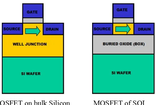
MOSFET on bulk Silicon MOSFET of SOI
Figure 2.1: Comparison of bulk and SOI structure
8
2.4 History of Silicon on Insulator
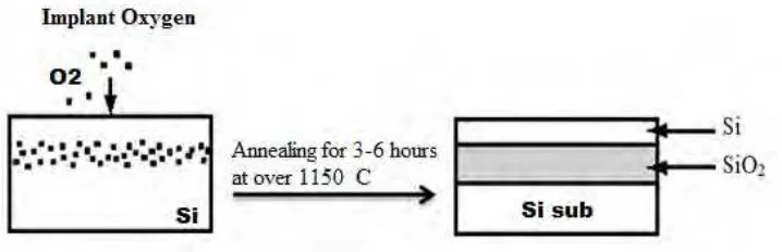
The introduction of Silicon on Insulator MOSFET start around sixth decade ago which is from 1960’s and the first implemented in the thin-film transistor (TFT). SOI device was born by the development of Separation by Implemented Oxygen (SIMOX) fabrication process by Watanabe and Tooi. They implement oxygen ion into silicon substrate using an RF gas discharge. In 1978, Izumi discover the way to produces a continues buried SiO2 layer with the excellent characteristic
by implantation of oxygen into silicon at an acceleration voltage 150 kV and a dose of 1.2 1018 cm-2 with the annealing temperature of 1150 C. This process
will left a thin layer of single-crystal silicon on the surface [1].
Figure 2.2: SIMOX Process
In early 80s, intensive research on the technique of recrystallization with laser or e-beam. It turned out, however, to be possible circumvent photolithography limitation by using a shorter wavelength of the light source [13]. In the middle 80s Fully-depleted SOI MOSFET began attracting attention because of their advantage. Engineers concentrate analysis of drain breakdown phenomena and improvement of the drain breakdown voltage [1].