i
REALISASI DAN ANALISIS PORTABLE SOLAR CHARGER
Nama : Yuhlianto Nugraha
NRP : 0822006
Jurusan Teknik Elektro, Fakultas Teknik, Universitas Kristen Maranatha
Jl. Prof. Drg. Suria Sumantri, MPH. no. 65, Bandung, Indonesia
Email :
ABSTRAK
Alat elektronik yang bersifat portable memiliki masalah yakni ketahanan
asupan energi listriknya, karena alat elektronik tersebut mendapat energi dari baterai
yang mempunyai keterbatasan kapasitas penyimpanan energi listrik bila dibandingkan
dengan listrik PLN.
Pada tugas akhir ini direalisasikan suatu portable charger yang menggunakan
prinsip kerja rangkaian-rangkaian DC-DC converter seperti: buck converter, boost
converter dan buck-boost converter. Untuk sumber energi listriknya digunakan sel
surya dan baterai pendukung. Setelah itu karakteristiknya dianalisis.
Berdasarkan hasil percobaan, portable charger ini dapat mengisi baterai
handphone dengan efisiensi rata-rata 78.78%.
Kata kunci: portable charger, buck converter, boost converter, buck-boost
ii
REALIZATION AND ANALYSIS of PORTABLE SOLAR
CHARGER
Name : Yuhlianto Nugraha
NRP : 0822006
Department of Electrical Engineering, Maranatha Christian University
Jl. Prof. Drg. Suria Sumantri, MPH. no. 65, Bandung, Indonesia
Email :
ABSTRACT
Portable electronic devices have some problem at endurance of electricity
supply, since these devices get energy from battery which has limited storage of
electricity capacity if it compares with PLN’s electricity
In this final assignment it has been realized a portable charger which using
DC-DC converter circuits principal such as: buck converter, boost converter and
buck-boost converter. For its power supply it is used solar cell and back-up battery.
After that, the performance will be analyzed.
According to e
xperiment result, this portable charger can charge handphone’s
battery with efficiency 78.78%.
Key word: portable charger, buck converter, boost converter, buck-boost converter,
v
DAFTAR ISI
ABSTRAK ... i
ABSTRACT ...ii
KATA PENGANTAR ... iii
DAFTAR ISI ... v
DAFTAR TABEL ... viii
DAFTAR GAMBAR ... x
BAB I
PENDAHULUAN ... 1
1.1
Latar Belakang. ... 1
1.2
Rumusan Masalah. ... 1
1.3
Tujuan ... 2
1.4
Batasan Masalah... 2
1.5
Spesifikasi Alat yang Dibuat ... 2
1.6
Sistematika. ... 3
BAB II
LANDASAN TEORI ... 4
2.1
Buck Converter ... 6
2.1.1
Continuous Mode ... 8
2.1.2
Discontinuous Mode ... 9
2.2
Boost Converter ... 11
2.2.1
Continuous Mode ... 13
2.2.2
Discontinuous Mode ... 14
2.3
Buck-boost converter. ... 15
2.3.1
Continuous Mode ... 17
BAB III
PERANCANGAN DAN REALISASI SOLAR CHARGER
PORTABLE ... 26
3.1
Diagram Blok ... 26
vi
3.3
Sel surya (Solar Cell) ... 27
3.4
LM2575 ... 28
3.4.1
Buck-boost converter ... 29
3.4.2
Perancangan Buck-boost converter ... 30
3.4.3
Buck Converter... 32
3.4.4
Perancangan Buck Converter ... 32
3.5
LM2577 ... 35
3.6
Back-up battery ... 41
3.7
Rangkaian Proteksi... 42
3.8
Rangkaian Indikator Tegangan Baterai ... 44
BAB IV
DATA PENGAMATAN DAN ANALISIS DATA ... 49
4.1
Buck-boost converter ... 49
4.2
Beban 150Ω
... 50
4.3
Beban 270Ω
... 51
4.4
Beban 420Ω
... 52
4.5
Beban Back-up battery ... 55
4.6
Intensitas 44200 Lux ... 55
4.7
Intensitas 53500 Lux. ... 55
4.4
Intensitas 67800 Lux ... 56
4.5
Intensitas 74400 Lux ... 56
4.6
Intensitas 83900 Lux ... 57
4.7
Intensitas 96400 Lux. ... 57
4.6
Intensitas 118600 Lux ... 58
4.2
Buck Converter. ... 61
4.2.1
Nokia 1325 CDMA ... 61
4.2.2
Huawei C2061 ... 69
4.2.3
Analisis Buck Converter ... 77
4.3
Boost Converter ... 78
vii
BAB V KESIMPULAN DAN SARAN ... 82
5.1
KESIMPULAN ... 82
5.2
SARAN ... 82
DAFTAR PUSTAKA ... 84
LAMPIRAN A ...A-1
viii
Daftar Tabel
Tabel II.1 Perbandingan Efisiensi Berbagai Jenis Sel Surya ... 25
Tabel III.1 Spesifikasi Back-up battery REMCO 12V 1300mAH ... 41
Tabel IV.1 Buck-
boost converter ketika diberi dummy load sebesar 150Ω
.. ... 50
Tabel IV.2 Buck-
boost converter ketika diberi dummy load sebesar 270Ω
... 51
Tabel IV.3 Buck-
boost converter ketika diberi dummy load sebesar 420Ω
... 52
Tabel IV.4 Karakteristik rangkaian buck-boost converter saat intensitas cahaya
44200 lux... ... 55
Tabel IV.5 Karakteristik rangkaian buck-boost converter saat intensitas cahaya
53500 lux... ... 56
Tabel IV.6 Karakteristik rangkaian buck-boost converter saat intensitas cahaya
67800 lux... ... 56
Tabel IV.7 Karakteristik rangkaian buck-boost converter saat intensitas cahaya
74400 lux... ... 57
Tabel IV.8 Karakteristik rangkaian buck-boost converter saat intensitas cahaya
83900 lux... ... 57
Tabel IV.9 Karakteristik rangkaian buck-boost converter saat intensitas cahaya
96400 lux... ... 58
Tabel IV.10 Karakteristik rangkaian buck-boost converter saat intensitas cahaya
118600 lux.. ... 58
Tabel IV.11 Hasil ke-1 Buck Converter pada Nokia 1325 CDMA ... 62
Tabel IV.12 Hasil ke-2 Buck Converter pada Nokia 1325 CDMA ... 63
Tabel IV.13 Hasil ke-3 Buck Converter pada Nokia 1325 CDMA.. ... 64
Tabel IV.14 Hasil ke-4 Buck Converter pada Nokia 1325 CDMA ... 65
Tabel IV.15 Hasil ke-5 Buck Converter pada Nokia 1325 CDMA ... 66
Tabel IV.16 Hasil ke-1 Buck Converter pada Huawei C2601.. ... 70
Tabel IV.17 Hasil ke-2 Buck Converter pada Huawei C2601 ... 71
Tabel IV.18 Hasil ke-3 Buck Converter pada Huawei C2601 ... 72
ix
Tabel IV.20 Hasil ke-5 Buck Converter pada Huawei C2601.. ... 74
Tabel IV.21 Hasil Pengisian dengan Charger Asli ... 77
Tabel IV.22 Hasil Percobaan Boost Converter dengan beban berupa beberapa
x
Daftar Gambar
Gambar II.1 Buck Converter
[9]... 6
Gambar II.2 ON State Buck Converter
[9]... 6
Gambar II.3 OFF State Buck Converter
[9].. ... 6
Gambar II.4 Continuous Mode Buck Converter
[9]... 8
Gambar II.5 Discontinuous Mode Buck Converter ... 9
Gambar II.6 Boost Converter
[10]... 11
Gambar II.7 ON State Boost Converter ... 11
Gambar II.8 OFF State Boost Converter ... 11
Gambar II.9 Continuous Mode Boost Converter ... 13
Gambar II.10 Discontinuous Mode Boost Converter ... 14
Gambar II.11 Buck-boost converter
[8]... 15
Gambar II.12 ON State Buck-Boost ... 16
Gambar II.13 OFF State Buck-Boost.. ... 16
Gambar II.14 Continuous Mode Buck-boost converter ... 17
Gambar II.15 Discontinuous Mode Buck-boost converter ... 19
Gambar II.16 Struktur dasar dan mekanisme kerja sel surya silicon ... 22
Gambar II.17 Monocrystalline Silicon... 23
Gambar II.18 Polycristalline Silicon ... 24
Gambar II.19 Amorphous Silicon ... 25
Gambar III.1 Diagram Blok Solar Charger Portable ... 26
Gambar III.2 Sel Surya Bulk Monocristalline ... 28
Gambar III.3 Rangkaian Buck-Boost Converter Menggunakan LM2575 ... 30
Gambar III.4 Rangkaian Buck-Boost Converter Hasil Perancangan ... 31
Gambar III.5 Buck-boost converter ... 31
Gambar III.6 Rangkaian Buck Converter dengan IC LM2575
[5]... 32
Gambar III.7 Petunjuk Pemilihan Induktor untuk Buck Converter ... 33
Gambar III.8 Rangkaian Buck Converter Hasil Perancangan ... 34
xi
Gambar III.10 Rangkaian Boost Converter dengan IC LM2577
[4]... 36
Gambar III.11 Petunjuk Pemilihan Induktor untuk Boost Converter ... 38
Gambar III.12 Rangkaian Boost Converter Menggunakan LM2577 ... 40
Gambar III.13 Boost Converter ... 40
Gambar III.14 Back-up battery REMCO 12V 1300mAh ... 41
Gambar III.15 Rangkaian Proteksi
[6]... 43
Gambar III.16 Rangkaian Indikator Tegangan Baterai ... 45
Gambar III.17 Indikator Tegangan Baterai ... 45
Gambar III.18 Indikator Ketika Tegangan Baterai 5 Volt ... 46
Gambar III.19 Indikator Ketika Tegangan Baterai 10 Volt ... 47
Gambar III.20 Indikator Ketika Tegangan Baterai 14 Volt ... 47
Gambar III.21 Rangkaian Keseluruhan ... 48
Gambar IV.1 Proses Pengambilan Data Buck-boost converter ... 49
Gambar IV.2 Titik-titik Pengambilan Data pada Buck-boost converter ... 53
Gambar IV.
3 Bentuk Sinyal pada Titik A dengan V/div=2 dan Time/div=5μs
... 53
Gambar IV.4 B
entuk Sinyal pada Titik B dengan V/div=5 dan Time/div=0.5μs
... 54
Gambar IV.5 Bentuk Sinyal pada Titik C dengan V/div=5 ... 54
Gambar IV.6 Bentuk Sinyal Buck-Boost Converter pada Titik A dengan V/div=2
dan Time/div=10μs
... 59
Gambar IV.7 Bentuk Sinyal Buck-boost converter pada Titik B dengan V/div=5
dan Time/div=5μs
... 59
Gambar IV. 8 Bentuk Sinyal Buck-boost converter pada Titik C dengan
V/div=5...60
Gambar IV.9 Proses pengambilan data Buck
Converter...61
Gambar IV.10 Titik-Titik Pengamatan Bentuk Sinyal pada Buck Converter ... 67
Gambar IV.11 Bentuk Sinyal Buck Converter pada titik A dengan V/div=5 dan
Time/div=0.02ms ... 67
xii
Gambar IV.13 Bentuk Sinyal Buck Converter pada titik C dengan V/div=2 dan
Time/div=20μs
... 68
Gambar IV.14 Bentuk Sinyal Buck Converter pada Titik A dengan V/div=1 dan
Time/div
=50μs
... 75
Gambar IV.15 Bentuk Sinyal Buck Converter pada Titik B dengan V/div=2 dan
Time/div=0.5μs
... 76
Gambar IV.16 Bentuk Sinyal Buck Converter pada Titik C dengan V/div=2 dan
Time/div=10μs
... 76
Gambar IV.17 Titik-Titik Pengambilan Data pada Boost Converter ... 79
Gambar IV. 18 Bentuk Sinyal Boost Converter pada Titik A dengan V/div=5 ... 80
Gambar IV. 19 Bentuk Sinyal Boost Converter pada Titik B dengan V/div=2 dan
Time/div=10μs
... 80
Gambar IV. 20 Bentuk Sinyal Boost Converter pada Titik C dengan V/div=2 dan
Time/div=10μs
... 80
LAMPIRAN A
A - 1
Tampak Atas
Tampak Depan
A - 2
Tampak Belakang
LAMPIRAN B
DATASHEET
LM 2575……….B
-1
LM 2577……….B
-12
B- 1
LM1575/LM2575/LM2575HV
SIMPLE SWITCHER
®
1A Step-Down Voltage Regulator
General Description
The LM2575 series of regulators are monolithic integrated circuits that provide all the active functions for a step-down (buck) switching regulator, capable of driving a 1A load with excellent line and load regulation. These devices are avail- able in fixed output voltages of 3.3V, 5V, 12V, 15V, and an adjustable output version.
Requiring a minimum number of external components, these regulators are simple to use and include internal frequency compensation and a fixed-frequency oscillator.
The LM2575 series offers a high-efficiency replacement for popular three-terminal linear regulators. It substantially re- duces the size of the heat sink, and in many cases no heat sink is required.
A standard series of inductors optimized for use with the LM2575 are available from several different manufacturers. This feature greatly simplifies the design of switch-mode pow- er supplies.
Other features include a guaranteed ±4% tolerance on output voltage within specified input voltages and output load con- ditions, and ±10% on the oscillator frequency. External shut- down is included, featuring 50 μA (typical) standby current. The output switch includes cycle-by-cycle current limiting, as well as thermal shutdown for full protection under fault con- ditions.
Typical Application
(Fixed Output Voltage Versions)
Features
■
3.3V, 5V, 12V, 15V, and adjustable output versions
■
Adjustable version output voltage range,
1.23V to 37V (57V for HV version) ±4% max over line and load conditions
■
Guaranteed 1A output current
■
Wide input voltage range, 40V up to 60V for HV version
■
Requires only 4 external components
■
52 kHz fixed frequency internal oscillator
■
TTL shutdown capability, low power standby mode
■
High efficiency
■
Uses readily available standard inductors
■
Thermal shutdown and current limit protection
■
P+ Product Enhancement tested
Applications
■
Simple high-efficiency step-down (buck) regulator
■
Efficient pre-regulator for linear regulators
■
On-card switching regulators
■
Positive to negative converter (Buck-Boost)
B- 2
Block Diagram and Typical Application
3.3V, R2 = 1.7k 5V, R2 = 3.1k 12V, R2 = 8.84k 15V, R2 = 11.3k For ADJ. Version
R1 = Open, R2 = 0Ω
Note: Pin numbers are for the TO-220 package.
1147502
B- 3
Connection Diagrams
(XX indicates output voltage option. See Ordering Information table for complete part number.)
Straight Leads 5–Lead TO-220 (T)
Bent, Staggered Leads 5-Lead TO-220 (T)
Side View
1147524
Top View
1147522
Top View
1147523 LM2575T-XX Flow LB03 or
LM2575HVT-XX Flow LB03 LM2575T-XX or LM2575HVT-XX
See NS Package Number T05A
See NS Package Number T05D
16–Lead DIP (N or J) 24-Lead Surface Mount (M)
*No Internal Connection
Top View
1147525
1147526
LM2575N-XX or LM2575HVN-XX See NS Package Number N16A
LM1575J-XX-QML
*No Internal Connection
Top View
See NS Package Number J16A LM2575M-XX or LM2575HVM-XX
See NS Package Number M24B
TO-263(
S)
5-Lead Surface-Mount Package
B- 4
LM1575-ADJ, LM2575-ADJ,
LM2575HV-ADJ Electrical Characteristics
Specifications with standard type face are for TJ= 25°C, and those with boldface type apply over full Operating Temperature Range.
Symbol Parameter Conditions Typ LM1575-ADJ LM2575-ADJ
LM2575HV-ADJ Units (Limits) Limit (Note 2) Limit (Note 3)
SYSTEM PARAMETERS (Note 4) Test Circuit Figure 2
VOUT Feedback Voltage VIN = 12V, ILOAD = 0.2A VOUT = 5V
Circuit of Figure 2
1.230 1.217 1.243 1.217 1.243 V V(Min) V(Max) VOUT Feedback Voltage
LM1575/LM2575
0.2A
≤
ILOAD≤
1A,8V
≤
VIN≤
40VV = 5V, Circuit of Figure 2
1.230 1.205/1.193 1.255/1.267 1.193/1.180 1.267/1.280 V V(Min) V(Max) VOUT Feedback Voltage
LM2575HV
0.2A
≤
ILOAD≤
1A,8V
≤
VIN≤
60VV = 5V, Circuit of Figure 2
1.230 1.205/1.193 1.261/1.273 1.193/1.180 1.273/1.286 V V(Min) V(Max)
η Efficiency VIN = 12V, ILOAD = 1A, VOUT = 5V 77
%
All Output Voltage Versions
Electrical Characteristics
Specifications with standard type face are for TJ = 25°C, and those with boldface type apply over full Operating Temperature Range. Unless otherwise specified, VIN = 12V for the 3.3V, 5V, and Adjustable version, VIN = 25V for the 12V version, and VIN = 30V for the 15V version. ILOAD = 200 mA.
Symbol Parameter Conditions Typ LM1575-XX LM2575-XX
LM2575HV-XX Units (Limits) Limit (Note 2) Limit (Note 3) DEVICE PARAMETERS
Ib Feedback Bias Current VOUT = 5V (Adjustable Version Only) 50 100/500 100/500 nA
fO Oscillator Frequency (Note 13) 52
47/43 58/62 47/42 58/63 kHz kHz(Min) kHz(Max)
VSAT Saturation Voltage IOUT = 1A (Note 5) 0.9
1.2/1.4 1.2/1.4
V V(Max)
DC Max Duty Cycle (ON) (Note 6) 98
93 93
%
%(Min)
ICL Current Limit Peak Current (Notes 5, 13) 2.2
1.7/1.3 3.0/3.2 1.7/1.3 3.0/3.2 A A(Min) A(Max) IL Output Leakage
Current
(Notes 7, 8) Output = 0V
Output = −1V
Output = −1V 7.5
2 30 2 30 mA(Max) mA mA(Max)
IQ Quiescent Current (Note 7) 5
10/12 10
mA mA(Max)
ISTBY Standby Quiescent
Current
ON /OFF Pin = 5V (OFF) 50
200/500 200
μ A
B- 5
Inductor Value Selection Guides
(For Continuous Mode Operation)
FIGURE 3. LM2575(HV)-3.3
1147510
FIGURE 5. LM2575(HV)-12
1147512
FIGURE 4. LM2575(HV)-5.0
1147511
FIGURE 6. LM2575(HV)-15
1147513
1147514
B- 6
PROCEDURE (Adjustable Output Voltage Versions) EXAMPLE (Adjustable Output Voltage Versions) Given:
VOUT = Regulated Output Voltage VIN(Max) = Maximum Input Voltage ILOAD(Max) = Maximum Load Current F = Switching Frequency (Fixed at 52 kHz)
Given:
VOUT = 10V VIN(Max) = 25V ILOAD(Max) = 1A F = 52 kHz
1. Programming Output Voltage (Selecting R1 and R2, as shown 1.Programming Output Voltage (Selecting R1 and R2)
in Figure 2 )
Use the following formula to select the appropriate resistor values.
R1 can be between 1k and 5k. (For best temperature coefficient and stability with time, use 1% metal film resistors)
2. Inductor Selection (L1)
A. Calculate the inductor Volt • microsecond constant, E • T (V •μ s), from the following formula:
R2 = 1k (8.13 − 1) = 7.13k, closest 1% value is 7.15k
2. Inductor Selection (L1)
A. Calculate E • T (V • μ s)
B. E • T = 115 V • μ s
B. Use the E • T value from the previous formula and match it with C. I
LOAD(Max) = 1A
the E • T number on the vertical axis of the Inductor Value Selec-tion Guide shown in Figure 7.
C. On the horizontal axis, select the maximum load current.
D. Identify the inductance region intersected by the E • T value and the maximum load current value, and note the inductor code for that region.
E. Identify the inductor value from the inductor code, and select an appropriate inductor from the table shown in Figure 9. Part numbers are listed for three inductor manufacturers. The inductor chosen must be rated for operation at the LM2575 switching frequency (52 kHz) and for a current rating of 1.15 × ILOAD. For additional inductor information, see the inductor section in the application hints section of this data sheet.
3. Output Capacitor Selection (COUT)
D. Inductance Region = H470
E. Inductor Value = 470 μH Choose from AIE part #430-0634,
Pulse Engineering part #PE-53118, or Renco part #RL-1961.
3. Output Capacitor Selection (COUT) A. The value of the output capacitor together with the inductor de- A.
fines the dominate pole-pair of the switching regulator loop. For stable operation, the capacitor must satisfy the following require- ment:
The above formula yields capacitor values between 10 μ F and 2000
B- 7
PROCEDURE (Adjustable Output Voltage Versions) EXAMPLE (Adjustable Output Voltage Versions) 4. Catch Diode Selection (D1)
A. The catch-diode current rating must be at least 1.2 times greater than the maximum load current. Also, if the power supply design must withstand a continuous output short, the diode should have a current rating equal to the maximum current limit of the LM2575. The most stressful condition for this diode is an overload or shorted output. See diode selection guide in Figure 8.
B. The reverse voltage rating of the diode should be at least 1.25 times the maximum input voltage.
5. Input Capacitor (CIN)
An aluminum or tantalum electrolytic bypass capacitor located close to the regulator is needed for stable operation.
4. Catch Diode Selection (D1)
A. For this example, a 3A current rating is adequate.
B. Use a 40V MBR340 or 31DQ04 Schottky diode, or any of the suggested fast-recovery diodes in Figure 8.
5. Input Capacitor (CIN)
A 100 μF aluminum electrolytic capacitor located near the input and ground pins provides sufficient bypassing.
B- 8
VR Schottky Fast Recovery
1A 3A 1A 3A
20V 1N5817 MBR120P SR102 1N5820 MBR320 SR302
The following diodes are all rated to 100V
11DF1 MUR110 HER102
The following diodes are all rated to 100V
31DF1 MURD310 HER302 30V 1N5818 MBR130P 11DQ03 SR103 1N5821 MBR330 31DQ03 SR303 40V 1N5819 MBR140P 11DQ04 SR104 IN5822 MBR340 31DQ04 SR304 50V MBR150 11DQ05 SR105 MBR350 31DQ05 SR305 60V MBR160 11DQ06 SR106 MBR360 31DQ06 SR306
FIGURE 8. Diode Selection Guide Inductor Code Inductor Value Schott (Note 15) Pulse Eng. (Note 16) Renco (Note 17)
L100 100 μH 67127000 PE-92108 RL2444
L150 150 μH 67127010 PE-53113 RL1954
L220 220 μH 67127020 PE-52626 RL1953
L330 330 μH 67127030 PE-52627 RL1952
L470 470 μH 67127040 PE-53114 RL1951
L680 680 μH 67127050 PE-52629 RL1950
H150 150 μH 67127060 PE-53115 RL2445
H220 220 μH 67127070 PE-53116 RL2446
H330 330 μH 67127080 PE-53117 RL2447
H470 470 μH 67127090 PE-53118 RL1961
H680 680 μH 67127100 PE-53119 RL1960
H1000 1000
μ
67127110 PE-53120 RL1959
H1500 1500
μ
67127120 PE-53121 RL1958
H2200 2200
μH
67127130 PE-53122 RL2448
Note 15: Schott Corp., (612) 475-1173, 1000 Parkers Lake Rd., Wayzata, MN 55391.
Note 16: Pulse Engineering, (619) 674-8100, P.O. Box 12236, San Diego, CA 92112.
Note 17: Renco Electronics Inc., (516) 586-5566, 60 Jeffryn Blvd. East, Deer Park, NY 11729.
B- 9
Application Hints
INPUT CAPACITOR (CIN)
To maintain stability, the regulator input pin must be bypassed with at least a 47 μF electrolytic capacitor. The capacitor's leads must be kept short, and located near the regulator.
If the operating temperature range includes temperatures be- low −25°C, the input capacitor value may need to be larger. With most electrolytic capacitors, the capacitance value de- creases and the ESR increases with lower temperatures and age. Paralleling a ceramic or solid tantalum capacitor will in- crease the regulator stability at cold temperatures. For maxi- mum capacitor operating lifetime, the capacitor's RMS ripple current rating should be greater than
INDUCTOR SELECTION
All switching regulators have two basic modes of operation: continuous and discontinuous. The difference between the two types relates to the inductor current, whether it is flowing continuously, or if it drops to zero for a period of time in the normal switching cycle. Each mode has distinctively different operating characteristics, which can affect the regulator per- formance and requirements.
The LM2575 (or any of the Simple Switcher family) can be used for both continuous and discontinuous modes of oper- ation.
The inductor value selection guides in Figure 3 through Figure 7 were designed for buck regulator designs of the continuous inductor current type. When using inductor values shown in the inductor selection guide, the peak-to-peak inductor ripple current will be approximately 20% to 30% of the maximum DC current. With relatively heavy load currents, the circuit oper- ates in the continuous mode (inductor current always flowing), but under light load conditions, the circuit will be forced to the discontinuous mode (inductor current falls to zero for a period of time). This discontinuous mode of operation is perfectly acceptable. For light loads (less than approximately 200 mA) it may be desirable to operate the regulator in the discontin-
uous mode, primarily because of the lower inductor values required for the discontinuous mode.
The selection guide chooses inductor values suitable for con- tinuous mode operation, but if the inductor value chosen is prohibitively high, the designer should investigate the possi-
circuits, or can give incorrect scope readings because of in- duced voltages in the scope probe.
The inductors listed in the selection chart include ferrite pot core construction for AIE, powdered iron toroid for Pulse En- gineering, and ferrite bobbin core for Renco.
An inductor should not be operated beyond its maximum rat- ed current because it may saturate. When an inductor begins to saturate, the inductance decreases rapidly and the inductor begins to look mainly resistive (the DC resistance of the wind- ing). This will cause the switch current to rise very rapidly. Different inductor types have different saturation characteris- tics, and this should be kept in mind when selecting an in- ductor.
The inductor manufacturer's data sheets include current and energy limits to avoid inductor saturation.
INDUCTOR RIPPLE CURRENT
When the switcher is operating in the continuous mode, the inductor current waveform ranges from a triangular to a saw- tooth type of waveform (depending on the input voltage). For a given input voltage and output voltage, the peak-to-peak amplitude of this inductor current waveform remains constant. As the load current rises or falls, the entire sawtooth current waveform also rises or falls. The average DC value of this waveform is equal to the DC load current (in the buck regu- lator configuration).
If the load current drops to a low enough level, the bottom of the sawtooth current waveform will reach zero, and the switcher will change to a discontinuous mode of operation. This is a perfectly acceptable mode of operation. Any buck switching regulator (no matter how large the inductor value is) will be forced to run discontinuous if the load current is light enough.
OUTPUT CAPACITOR
An output capacitor is required to filter the output voltage and is needed for loop stability. The capacitor should be located near the LM2575 using short pc board traces. Standard alu- minum electrolytics are usually adequate, but low ESR types are recommended for low output ripple voltage and good sta- bility. The ESR of a capacitor depends on many factors, some which are: the value, the voltage rating, physical size and the type of construction. In general, low value or low voltage (less than 12V) electrolytic capacitors usually have higher ESR numbers.
The amount of output ripple voltage is primarily a function of the ESR (Equivalent Series Resistance) of the output capac- itor and the amplitude of the inductor ripple current (ΔIIND).
See the section on inductor ripple current in Application Hints. The lower capacitor values (220 μ F–680 μ F) will allow typi- cally 50 mV to 150 mV of output ripple voltage, while larger- value capacitors will reduce the ripple to approximately 20 mV to 50 mV.
bility of discontinuous operation. The computer design soft-
B- 10
values for discontinuous (as well as continuous) mode of op- eration.
Inductors are available in different styles such as pot core, toriod, E-frame, bobbin core, etc., as well as different core materials, such as ferrites and powdered iron. The least ex- pensive, the bobbin core type, consists of wire wrapped on a ferrite rod core. This type of construction makes for an inex- pensive inductor, but since the magnetic flux is not completely contained within the core, it generates more electromagnetic interference (EMI). This EMI can cause problems in sensitive readily conducted through the leads to the printed circuit board copper, which is acting as a heat sink
For best thermal performance, the ground pins and all the unconnected pins should be soldered to generous amounts of printed circuit board copper, such as a ground plane. Large areas of copper provide the best transfer of heat to the sur- rounding air. Copper on both sides of the board is also helpful in getting the heat away from the package, even if there is no direct copper contact between the two sides. Thermal resis-
tance numbers as low as 40°C/W for the SO package, and 30°C/W for the N package can be realized with a carefully engineered pc board.
Included on the Switchers Made Simple design software is a more precise (non-linear) thermal model that can be used to determine junction temperature with different input-output parameters or different component values. It can also calcu- late the heat sink thermal resistance required to maintain the regulators junction temperature below the maximum operat- ing temperature.
Additional Applications
INVERTING REGULATOR
Figure 10 shows a LM2575-12 in a buck-boost configuration to generate a negative 12V output from a positive input volt- age. This circuit bootstraps the regulator's ground pin to the negative output voltage, then by grounding the feedback pin, the regulator senses the inverted output voltage and regu- lates it to −12V.
For an input voltage of 12V or more, the maximum available output current in this configuration is approximately 0.35A. At lighter loads, the minimum input voltage required drops to approximately 4.7V.
The switch currents in this buck-boost configuration are high- er than in the standard buck-mode design, thus lowering the available output current. Also, the start-up input current of the buck-boost converter is higher than the standard buck-mode regulator, and this may overload an input power source with a current limit less than 1.5A. Using a delayed turn-on or an undervoltage lockout circuit (described in the next section)
would allow the input voltage to rise to a high enough level before the switcher would be allowed to turn on.
Because of the structural differences between the buck and the buck-boost regulator topologies, the buck regulator de- sign procedure section can not be used to select the inductor or the output capacitor. The recommended range of inductor values for the buck-boost design is between 68 μH and 220 μH, and the output capacitor values must be larger than what is normally required for buck designs. Low input voltages or high output currents require a large value output capacitor (in the thousands of micro Farads).
The peak inductor current, which is the same as the peak switch current, can be calculated from the following formula:
Where fosc = 52 kHz. Under normal continuous inductor cur- rent operating conditions, the minimum VIN represents the worst case. Select an inductor that is rated for the peak cur- rent anticipated.
Also, the maximum voltage appearing across the regulator is the absolute sum of the input and output voltage. For a −12V output, the maximum input voltage for the LM2575 is +28V, or +48V for the LM2575HV.
The Switchers Made Simple (version 3.3) design software can be used to determine the feasibility of regulator designs using different topologies, different input-output parameters, different components, etc.
1147515
B- 12
LM1577/LM2577
SIMPLE SWITCHER
®
Step-Up Voltage Regulator
April 2005
General Description
The LM1577/LM2577 are monolithic integrated circuits that provide all of the power and control functions for step-up (boost), flyback, and forward converter switching regulators. The device is available in three different output voltage versions: 12V, 15V, and adjustable.
Requiring a minimum number of external components, these regulators are cost effective, and simple to use. Listed in this data sheet are a family of standard inductors and flyback transformers designed to work with these switching regula- tors.
Included on the chip is a 3.0A NPN switch and its associated protection circuitry, consisting of current and thermal limiting, and undervoltage lockout. Other features include a 52 kHz fixed-frequency oscillator that requires no external compo- nents, a soft start mode to reduce in-rush current during start-up, and current mode control for improved rejection of input voltage and output load transients.
Features
n Requires few external components
n NPN output switches 3.0A, can stand off 65V n Wide input voltage range: 3.5V to 40V n Current-mode operation for improved transient
response, line regulation, and current limit n 52 kHz internal oscillator
n Soft-start function reduces in-rush current during start-up n Output switch protected by current limit, under-voltage
lockout, and thermal shutdown
Typical Applications
n Simple boost regulator n Flyback and forward regulators n Multiple-output regulator
Connection Diagrams
Straight Leads 5-Lead TO-220 (T)
Bent, Staggered Leads 5-Lead TO-220 (T)
Top View
01146804
Top View
01146805
Order Number LM2577T-12, LM2577T-15, or LM2577T-ADJ
See NS Package Number T05A
Order Number LM2577T-12 Flow LB03, LM2577T-15 Flow LB03, or LM2577T-ADJ Flow LB03
B- 13
Connection Diagrams
(Continued)16-Lead DIP (N) 24-Lead Surface Mount (M)
*No internal Connection
Top View
01146806
Order Number 12, LM2577N-15, or LM2577N-ADJ
See NS Package Number N16A 01146807
*No internal Connection
Top View
Order Number 12, LM2577M-15, or LM2577M-ADJ See NS Package Number M24B
TO-263 (S)
5-Lead Surface-Mount Package
Top View
01146832
01146833
Side View
Order Number LM2577S-12, LM2577S-15, or LM2577S-ADJ
See NS Package Number TS5B
4-Lead TO-3 (K)
Bottom View
01146808
B- 14
Ordering Information
Temperature Range
Package Type
Output Voltage NSC
12V 15V ADJ Package Package
Drawing
−40˚C TA +125˚C 24-Pin Surface LM2577M-12 LM2577M-15 LM2577M-ADJ M24B SO
Mount
16-Pin Molded DIP LM2577N-12 LM2577N-15 LM2577N-ADJ N16A N
5-Lead Surface LM2577S-12 LM2577S-15 LM2577S-ADJ TS5B TO-263
Mount
5-Straight Leads LM2577T-12 LM2577T-15 LM2577T-ADJ T05A TO-220
5-Bent Staggered LM2577T-12 LM2577T-15 LM2577T-ADJ T05D TO-220
Leads Flow LB03 Flow LB03 Flow LB03
−55˚CTA +150˚C 4-Pin TO-3 LM1577K-12/883LM1577K-15/883 LM1577K-
ADJ/883
K04A TO-3
Typical Application
Note: Pin numbers shown are for TO-220 (T) package.
B- 15
Absolute Maximum Ratings
(Note 1)If Military/Aerospace specified devices are required, please contact the National Semiconductor Sales Office/ Distributors for availability and specifications.
Supply Voltage 45V
Output Switch Voltage 65V
Output Switch Current (Note 2) 6.0A
Power Dissipation Internally Limited
Storage Temperature Range −65˚C to +150˚C Lead Temperature
(Soldering, 10 sec.) 260˚C
Maximum Junction Temperature 150˚C
Minimum ESD Rating
(C = 100 pF, R = 1.5 k) 2 kV
Operating Ratings
Supply Voltage 3.5V VIN 40V
Output Switch Voltage 0V VSWITCH 60V
Output Switch Current ISWITCH 3.0A
Junction Temperature Range
LM1577 −55˚CTJ +150˚C
LM2577 −40˚CTJ +125˚C
Electrical Characteristics
—
LM1577-12, LM2577-12
Specifications with standard type face are for TJ = 25˚C, and those in bold type face apply over full Operating Temperature Range. Unless otherwise specified, VIN = 5V, and ISWITCH = 0.
LM1577-12 LM2577-12 Units
Symbol Parameter Conditions Typical Limit Limit (Limits)
(Notes 3, 4) (Note 5)
SYSTEM PARAMETERS Circuit of Figure1(Note 6)
VOUT Output Voltage VIN = 5V to 10V 12.0
V
ILOAD = 100 mA to 800 mA 11.60/11.40 11.60/11.40 V(min)
(Note 3) 12.40/12.60 12.40/12.60 V(max)
Line Regulation VIN = 3.5V to 10V 20 mV
ILOAD = 300 mA 50/100 50/100 mV(max)
Load Regulation VIN = 5V 20
mV
ILOAD = 100 mA to 800 mA 50/100 50/100 mV(max)
Efficiency VIN = 5V, ILOAD = 800 mA 80 %
DEVICE PARAMETERS
IS Input Supply Current VFEEDBACK = 14V (Switch Off) 7.5 mA
10.0/14.0 10.0/14.0 mA(max)
ISWITCH = 2.0A 25 mA
VCOMP = 2.0V (Max Duty Cycle) 50/85 50/85 mA(max)
VUV Input Supply ISWITCH = 100 mA 2.90
V
Undervoltage Lockout
2.70/2.65 2.70/2.65 V(min)
3.10/3.15 3.10/3.15 V(max)
fO Oscillator Frequency Measured at Switch Pin 52 kHz
ISWITCH = 100 mA 48/42 48/42 kHz(min)
56/62 56/62 kHz(max)
VREF Output Reference Measured at Feedback Pin V
Voltage VIN = 3.5V to 40V 12 11.76/11.64 11.76/11.64 V(min)
VCOMP = 1.0V 12.24/12.36 12.24/12.36 V(max)
Output Reference VIN = 3.5V to 40V 7 mV
Voltage Line Regulator
RFB Feedback Pin Input 9.7 k
Resistance
GM Error Amp ICOMP = −30 µA to +30 µA 370 µmho
Transconductance VCOMP = 1.0V 225/145 225/145 µmho(min)
B- 16
Electrical Characteristics
—
LM1577-15, LM2577-15
(Continued)Specifications with standard type face are for TJ = 25˚C, and those in bold type face apply over full Operating Temperature Range. Unless otherwise specified, VIN = 5V, and ISWITCH = 0.
Symbol Parameter Conditions Typical
LM1577-15 Limit
(Notes 3, 4)
LM2577-15 Limit
(Note 5)
Units (Limits)
DEVICE PARAMETERS
NPN Switch Current Limit
VCOMP = 2.0V 4.3
3.7/3.0 5.3/6.0 3.7/3.0 5.3/6.0 A A(min) A(max)
Electrical Characteristics
—
LM1577-ADJ, LM2577-ADJ
Specifications with standard type face are for TJ = 25˚C, and those in bold type face apply over full Operating Temperature Range. Unless otherwise specified, VIN = 5V, VFEEDBACK = VREF, and ISWITCH = 0.
Symbol Parameter Conditions Typical
LM1577-ADJ Limit
(Notes 3, 4)
LM2577-ADJ Limit
(Note 5)
Units (Limits)
SYSTEM PARAMETERS Circuit of Figure3(Note 6) VOUT Output Voltage VIN = 5V to 10V
ILOAD = 100 mA to 800 mA
(Note 3)
12.0 11.60/11.40 12.40/12.60 11.60/11.40 12.40/12.60 V V(min) V(max)
VOUT/
VIN
Line Regulation VIN = 3.5V to 10V
ILOAD = 300 mA
20
50/100 50/100
mV mV(max)
VOUT/
ILOAD
Load Regulation VIN = 5V
ILOAD = 100 mA to 800 mA
20
50/100 50/100
mV mV(max)
Efficiency VIN = 5V, ILOAD = 800 mA 80 %
DEVICE PARAMETERS
IS Input Supply Current VFEEDBACK = 1.5V (Switch Off) 7.5
10.0/14.0 10.0/14.0
mA mA(max) ISWITCH = 2.0A
VCOMP = 2.0V (Max Duty Cycle)
25
50/85 50/85
mA mA(max)
VUV Input Supply
Undervoltage Lockout
ISWITCH = 100 mA 2.90
2.70/2.65 3.10/3.15 2.70/2.65 3.10/3.15 V V(min) V(max) fO Oscillator Frequency Measured at Switch Pin
ISWITCH = 100 mA
52 48/42 56/62 48/42 56/62 kHz kHz(min) kHz(max)
VREF Reference
Voltage
Measured at Feedback Pin VIN = 3.5V to 40V
VCOMP = 1.0V
1.230 1.214/1.206
1.246/1.254 1.214/1.206 1.246/1.254 V V(min) V(max)
VREF/
VIN
Reference Voltage Line Regulation
VIN = 3.5V to 40V 0.5 mV
IB Error Amp
Input Bias Current
VCOMP = 1.0V 100
300/800 300/800
nA nA(max)
GM Error Amp
Transconductance
ICOMP = −30 µA to +30 µA
VCOMP = 1.0V
3700 2400/1600 4800/5800 2400/1600 4800/5800 µmho µmho(min) µmho(max)
AVOL Error Amp
Voltage Gain
VCOMP = 1.1V to 1.9V
RCOMP = 1.0 M (Note 7)
800
500/250 500/250
V/V V/V(min)
Electrical Characteristics
—
LM1577-ADJ, LM2577-ADJ
(Continued)B- 17
Symbol Parameter Conditions Typical
LM1577-ADJ Limit
(Notes 3, 4)
LM2577-ADJ Limit
(Note 5)
Units (Limits)
DEVICE PARAMETERS
Error Amplifier Output Swing
Upper Limit
VFEEDBACK = 1.0V
2.4
2.2/2.0 2.2/2.0
V V(min) Lower Limit
VFEEDBACK = 1.5V
0.3
0.40/0.55 0.40/0.55
V V(max) Error Amp
Output Current
VFEEDBACK = 1.0V to 1.5V
VCOMP = 1.0V
±200
±130/
±
90±300/
±
400±130/
±
90±300/
±
400µA µA(min) µA(max) ISS Soft Start Current VFEEDBACK = 1.0V
VCOMP = 0V
5.0 2.5/1.5 7.5/9.5 2.5/1.5 7.5/9.5 µA µA(min) µA(max) D Maximum Duty Cycle VCOMP = 1.5V
ISWITCH = 100 mA
95
93/90 93/90
% %(min)
ISWITCH/
VCOMP
Switch
Transconductance
12.5
A/V
IL Switch Leakage
Current
VSWITCH = 65V
VFEEDBACK = 1.5V (Switch Off)
10
300/600 300/600
µA µA(max) VSAT Switch Saturation
Voltage
ISWITCH = 2.0A
VCOMP = 2.0V (Max Duty Cycle)
0.5
0.7/0.9 0.7/0.9
V V(max) NPN Switch
Current Limit
VCOMP = 2.0V 4.3
3.7/3.0 5.3/6.0 3.7/3.0 5.3/6.0 A A(min) A(max)
THERMAL PARAMETERS (All Versions)
JA
JC
Thermal Resistance K Package, Junction to Ambient K Package, Junction to Case
35 1.5
˚C/W
JA
JC
T Package, Junction to Ambient T Package, Junction to Case
65 2
JA N Package, Junction to
Ambient (Note 8)
85
JA M Package, Junction
to Ambient (Note 8)
100
JA S Package, Junction to
Ambient (Note 9)
B- 18
VApplication Hints
(Continued)STEP-UP (BOOST) REGULATOR
Figure 4 shows the LM1577-ADJ/LM2577-ADJ used as a Step-Up Regulator. This is a switching regulator used for
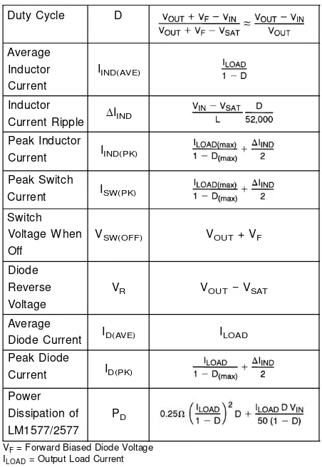
Duty Cycle D
Average producing an output voltage greater than the input supply
voltage. The LM1577-12/LM2577-12 and LM1577-15/ LM2577-15 can also be used for step-up regulators with 12V or 15V outputs (respectively), by tying the feedback pin directly to the regulator output.
A basic explanation of how it works is as follows. The LM1577/LM2577 turns its output switch on and off at a frequency of 52 kHz, and this creates energy in the inductor
Inductor Current Inductor Current Ripple Peak Inductor Current
Peak Switch
IIND(AVE)
IIND
IIND(PK)
(L). When the NPN switch turns on, the inductor current charges up at a rate of VIN/L, storing current in the inductor.
When the switch turns off, the lower end of the inductor flies
Current ISW(PK)
Switch above VIN, discharging its current through diode (D) into the
output capacitor (COUT) at a rate of (VOUT − VIN)/L. Thus,
energy stored in the inductor during the switch on time is transferred to the output during the switch off time. The output voltage is controlled by the amount of energy trans- ferred which, in turn, is controlled by modulating the peak inductor current. This is done by feeding back a portion of
Voltage When Off Diode Reverse Voltage Average
VSW(OFF) VOUT + VF
VR VOUT − VSAT
the output voltage to the error amp, which amplifies the difference between the feedback voltage and a 1.230V ref-
ID(AVE) ILOAD
Diode Current
erence. The error amp output voltage is compared to a voltage proportional to the switch current (i.e., inductor cur- rent during the switch on time).
The comparator terminates the switch on time when the two voltages are equal, thereby controlling the peak switch cur- rent to maintain a constant output voltage.
Peak Diode Current
Power Dissipation of LM1577/2577
ID(PK)
PD
Voltage and current waveforms for this circuit are shown in
Figure 5, and formulas for calculating them are given in
Figure6.
01146811
FIGURE 5. Step-Up Regulator Waveforms
VF = Forward Biased Diode Voltage
ILOAD = Output Load Current
FIGURE 6. Step-Up Regulator Formulas STEP-UP REGULATOR DESIGN PROCEDURE
The following design procedure can be used to select the appropriate external components for the circuit in Figure 4, based on these system requirements.
Given:
VIN (min) = Minimum input supply voltage
VOUT = Regulated output voltage
ILOAD(max) = Maximum output load current
Before proceeding any further, determine if the LM1577/ LM2577 can provide these values of VOUT and ILOAD(max)
when operating with the minimum value of VIN. The upper
limits for VOUT and ILOAD(max) are given by the following
equations.
VOUT 60V
and VOUT 10 x VIN(min)
These limits must be greater than or equal to the values specified in this application.
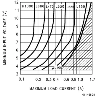
1. Inductor Selection (L)
A. VoltageOptions:
1. For 12V or 15V output
From Figure 7 (for 12V output) or Figure 8 (for 15V output), identify inductor code for region indicated by
[image:32.595.299.525.52.380.2] [image:32.595.75.247.412.573.2]B- 19
Application Hints
(Continued)ditions for which the LM1577/LM2577 output switch would be operating beyond its switch current rating. The minimum operating voltage for the LM1577/LM2577 is 3.5V.
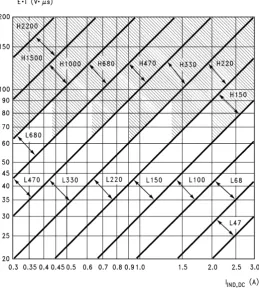
From here, proceedtostepC. 2. For Adjustable version Preliminary calculations:
The inductor selection is based on the calculation of the following three parameters:
D(max), the maximum switch duty cycle (0 D 0.9):
where VF = 0.5V for Schottky diodes and 0.8V for fast
recovery diodes (typically);
E •T, the product of volts x time that charges the inductor:
IIND,DC, the average inductor current under full load;
B. IdentifyInductorValue:
1. From Figure 9, identify the inductor code for the region indicated by the intersection of E•T and IIND,DC.
This code gives the inductor value in microhenries. The L or H prefix signifies whether the inductor is rated for a maximum E•T of 90 V•µs (L) or 250 V•µs (H).
2. If D < 0.85, go on to step C. If D 0.85, then calculate the minimum inductance needed to ensure the switching regulator’s stability:
If LMIN is smaller than the inductor value found in step B1, go
on to step C. Otherwise, the inductor value found in step B1 is too low; an appropriate inductor code should be obtained from the graph as follows:
1. Find the lowest value inductor that is greater than LMIN.
2. Find where E•T intersects this inductor value to determine if it has an L or H prefix. If E•T intersects both the L and H regions, select the inductor with an H prefix.
01146827
FIGURE 7. LM2577-12 Inductor Selection Guide
01146828
[image:33.595.371.535.99.262.2] [image:33.595.372.534.307.472.2]B- 20
Application Hints
(Continued)01146812
Note: These charts assume that the inductor ripple current inductor is approximately 20% to 30% of the average inductor current (when the regulator is under full load). Greater ripple current causes higher peak switch currents and greater output ripple voltage; lower ripple current is achieved with larger-value
inductors. The factor of 20 to 30% is chosen as a convenient balance between the two extremes.
FIGURE 9. LM1577-ADJ/LM2577-ADJ Inductor Selection Graph
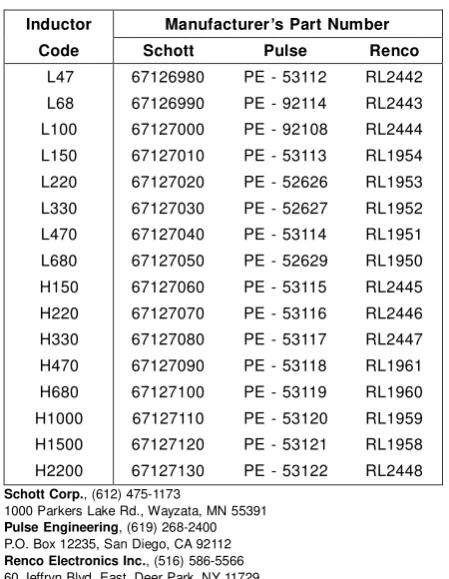
C. Select an inductor from the table of Figure 10 which cross-references the inductor codes to the
part numbers of three different manufacturers. Complete specifications for these inductors are available from the respective manufacturers. The inductors listed in this table have the following characteristics:
AIE: ferrite, pot-core inductors; Benefits of this type are low electro-magnetic interference (EMI), small physical size, and very low power dissipation (core loss). Be careful not to operate these inductors too far beyond their maximum ratings for E•T and peak current, as this will saturate the core.
Pulse:powdered iron, toroid core inductors; Benefits are low EMI and ability to withstand E•T and peak current above rated value better than ferrite cores.
[image:34.595.190.450.81.374.2]B- 21
Application Hints
(Continued)Inductor Code
Manufacturer’s Part Number
Schott Pulse Renco
L47 L68 L100 L150 L220 L330 L470 L680 H150 H220 H330 H470 H680 H1000 H1500 H2200
67126980 PE - 53112 RL2442 67126990 PE - 92114 RL2443 67127000 PE - 92108 RL2444 67127010 PE - 53113 RL1954 67127020 PE - 52626 RL1953 67127030 PE - 52627 RL1952 67127040 PE - 53114 RL1951 67127050 PE - 52629 RL1950 67127060 PE - 53115 RL2445 67127070 PE - 53116 RL2446 67127080 PE - 53117 RL2447 67127090 PE - 53118 RL1961 67127100 PE - 53119 RL1960 67127110 PE - 53120 RL1959 67127120 PE - 53121 RL1958 67127130 PE - 53122 RL2448
Schott Corp., (612) 475-1173
1000 Parkers Lake Rd., Wayzata, MN 55391
Pulse Engineering, (619) 268-2400 P.O. Box 12235, San Diego, CA 92112
Renco Electronics Inc., (516) 586-5566 60 Jeffryn Blvd. East, Deer Park, NY 11729
FIGURE 10. Table of Standardized Inductors and Manufacturer’s Part Numbers
C. CalculatetheminimumvalueofCC .
The compensation capacitor is also part of the soft start circuitry. When power to the regulator is turned on, the switch duty cycle is allowed to rise at a rate controlled by this capacitor (with no control on the duty cycle, it would imme- diately rise to 90%, drawing huge currents from the input power supply). In order to operate properly, the soft start circuit requires CC 0.22 µF.
The value of the output filter capacitor is normally large enough to require the use of aluminum electrolytic capaci- tors. Figure 11 lists several different types that are recom- mended for switching regulators, and the following param- eters are used to select the proper capacitor.
WorkingVoltage (WVDC):Choose a capacitor with a work- ing voltage at least 20% higher than the regulator output voltage.
Ripple Current:This is the maximum RMS value of current that charges the capacitor during each switching cycle. For step-up and flyback regulators, the formula for ripple current is
Choose a capacitor that is rated at least 50% higher than this value at 52 kHz.
Equivalent Series Resistance (ESR) : This is the primary cause of output ripple voltage, and it also affects the values of RC and CC needed to stabilize the regulator. As a result, 2. Compensation Network (RC, CC) and Output Capacitor
(COUT) Selection the preceding calculations for CC and RC
are only valid if
RC and CC form a pole-zero compensation network that
stabilizes the regulator. The values of RC and CC are mainly
dependant on the regulator voltage gain, ILOAD(max), L and
COUT. The following procedure calculates values for RC, CC,
and COUT that ensure regulator stability. Be aware that this
procedure doesn’t necessarily result in RC and CC that pro-
vide optimum compensation. In order to guarantee optimum compensation, one of the standard procedures for testing loop stability must be used, such as measuring VOUT tran-
sient response when pulsing ILOAD (see Figure15).
A. First,calculatethemaximumvalueforRC.
Select a resistor less than or equal to this value, and it should also be no greater than 3 k.
B. CalculatetheminimumvalueforCOUT using the following
two equations.
ESR doesn’t exceed the maximum value specified by the following equations.
Select a capacitor with ESR, at 52 kHz, that is less than or equal to the lower value calculated. Most electrolytic capaci- tors specify ESR at 120 Hz which is 15% to 30% higher than at 52 kHz. Also, be aware that ESR increases by a factor of 2 when operating at −20˚C.
In general, low values of ESR are achieved by using large value capacitors (C 470 µF), and capacitors with high WVDC, or by paralleling smaller-value capacitors.
[image:35.595.91.316.71.361.2]B- 22
VOUT (max)
Schottky Fast Recovery
1A 3A 1A 3A
20V 1N5817 MBR120P 1N5820 MBR320P 30V 1N5818 MBR130P 11DQ03 1N5821 MBR330P 31DQ03 40V 1N5819 MBR140P 11DQ04 1N5822 MBR340P 31DQ04 50V MBR150 11DQ05 MBR350 31DQ05 1N4933 MUR105 100V 1N4934 HER102 MUR110 10DL1 MR851 30DL1 MR831 HER302
Application Hints
(Continued)3. Output Voltage Selection (R1 and R2)
This section is for applications using the LM1577-ADJ/ LM2577-ADJ. Skip this section if the LM1577-12/LM2577-12 or LM1577-15/LM2577-15 is being used.
With the LM1577-ADJ/LM2577-ADJ, the output voltage is given by
VOUT = 1.23V (1 + R1/R2)
Resistors R1 and R2 divide the output down so it can be compared with the
LM1577-ADJ/LM2577-ADJ internal
1.23V reference. For a given desired output voltage VOUT, select R1 and R2 so that
4. Input Capacitor Selection (CIN)
The switching action in the step-up regulator causes a trian- gular ripple current to be drawn from the supply source. This in turn causes noise to appear on the supply voltage. For proper operation of the LM1577, the input voltage should be decoupled. Bypassing the Input Voltage pin directly to ground with a good quality, low ESR, 0.1 µF capacitor (leads as short as possible) is normally sufficient.
If the LM1577 is located far from the supply source filter capacitors, an additional large electrolytic capacitor (e.g. 47 µF) is often required.
5. Diode Selection (D)
The switching diode used in the boost regulator must with- stand a reverse voltage equal to the circuit output voltage, and must conduct the peak output current of the LM2577. A suitable diode must have a minimum reverse breakdown voltage greater than the circuit output voltage, and should be rated for average and peak current greater than ILOAD(max)
and ID(PK). Schottky barrier diodes are often favored for use
in switching regulators. Their low forward voltage drop allows higher regulator efficiency than if a (less expensive) fast recovery diode was used. See Figure12for recommended part numbers and voltage ratings of 1A and 3A diodes.
Cornell Dublier — Types 239, 250, 251, UFT,
300, or 350
P.O. Box 128, Pickens, SC 29671 (803) 878-6311
Nichicon — Types PF, PX, or PZ 927 East Parkway, Schaumburg, IL 60173
(708) 843-7500
Sprague — Types 672D, 673D, or 674D Box 1, Sprague Road, Lansing, NC 28643 (919) 384-2551
United Chemi-Con — Types LX, SXF, or SXJ
9801 West Higgins Road, Rosemont, IL 60018
(708) 696-2000
FIGURE 11. Aluminum Electrolytic Capacitors
Recommended for Switching Regulators
FIGURE 12. Diode Selection Chart
BOOST REGULATOR CIRCUIT EXAMPLE
By adding a few external components (as shown in Figure 13), the LM2577 can be used to produce a regulated output voltage that is greater than the applied input voltage. Typical performance of this regulator is shown in Figure 14 and
[image:36.595.303.524.221.431.2]B- 23
Application Hints
(Continued)FLYBACK REGULATOR
A Flyback regulator can produce single or multiple output voltages that are lower or greater than the input supply voltage. Figure 18 shows the LM1577/LM2577 used as a flyback regulator with positive and negative regulated out- puts. Its operation is similar to a step-up regulator, except the output switch contols the primary current of a flyback trans- former. Note that the primary and secondary windings are out of phase, so no current flows through secondary when current flows through the primary. This allows the primary to charge up the transformer core when the switch is on. When the switch turns off, the core discharges by sending current through the secondary, and this produces voltage at the outputs. The output voltages are controlled by adjusting the peak primary current, as described in the step-up regulator section.
Voltage and current waveforms for this circuit are shown in
Figure 17, and formulas for calculating them are given in
Figure19.
FLYBACK REGULATOR DESIGN PROCEDURE
1. Transformer Selection
A family of standardized flyback transformers is available for creating flyback regulators that produce dual output volt- ages, from ±10V to ±15V, as shown in Figure 18. Figure 20lists these transformers with the input voltage, output voltages and maximum load current they are designed for.
2. Compensation Network (CC, RC) and Output Capacitor (COUT) Selection
As explained in the Step-Up Regulator Design Procedure, CC, RC and COUT must be selected as a group. The following
procedure is for a dual output flyback regulator with equal turns ratios for each secondary (i.e., both output voltages have the same magnitude). The equations can be used for a single output regulator by changing ILOAD(max) to ILOAD(max)
in the following equations.
A. First, calculate the maximum value for RC.
Where ILOAD(max) is the sum of the load
current (magni- tude) required from both outputs. Select a resistor less than or equal to this value, and no greater than 3 k.
B. Calculate the minimum value for COUT (sum of
COUT
at both outputs) using the following two equations.
The larger of these two values must be used to ensure regulator stability.
01146817
[image:37.595.379.532.296.442.2]B- 24
LM3914
Dot/Bar
Display
Driver
General
Description
The LM3914 is a monolithic integrated circuit that senses analog voltage levels and drives 10 LEDs, providing a linear analog display. A single pin changes the display from a moving dot to a bar graph. Current drive to the LEDs is regulated and programmable, eliminating the need for resis- tors. This feature is one that allows operation of the whole system from less than 3V.
The circuit contains its own adjustable reference and accu- rate 10-step voltage divider. The low-bias-current input buffer accepts signals down to ground, or V−, yet needs no protection against inputs of 35V above or below ground. The buffer drives 10 individual comparators referenced to the precision divider. Indication non-linearity can thus be held typically to 1⁄2%, even over a wide temperature range.
Versatility was designed into the LM3914 so that controller, visual alarm, and expanded scale functions are easily added on to the display system. The circuit can drive LEDs of many colors, or low-current incandescent lamps. Many LM3914s can be “chained” to form displays of 20 to over 100 seg- ments. Both ends of the voltage divider are externally avail- able so that 2 drivers can be made into a zero-center meter. The LM3914 is very easy to apply as an analog meter circuit. A 1.2V full-scale meter requires only 1 resistor and a single 3V to 15V supply in addition to the 10 display LEDs. If the 1 resistor is a pot, it becomes the LED brightness control. The simplified block diagram illustrates this extremely simple external circuitry.
When in the dot mode, there is a small amount of overlap or
“fade” (about 1 mV) between segments. This assures that at
no time will all LEDs be “OFF”, and thus any ambiguous display is avoided. Various novel displays are possible.
February 2003
Much of the display flexibility derives from the fact that all outputs are individual, DC regulated currents. Various effects can be achieved by modulating these currents. The indi- vidual outputs can drive a transistor as well as a LED at the same time, so controller functions including “staging” control can be performed. The LM3914 can also act as a program- mer, or sequencer.
The LM3914 is rated for operation from 0˚C to +70˚C. The
LM3914N-1 is available in an 18-lead molded (N) package. The following typical application illustrates adjusting of the
reference to a desired value, and proper grounding for ac-
curate operation, and avoiding oscillations.
Features
n Drives LEDs, LCDs or vacuum fluorescents
n Bar or dot display mode externally selectable by user n Expandable to displays of 100 steps
n Internal voltage reference from 1.2V to 12V n Operates with single supply of less than 3V n Inputs operate down to ground
n Output current programmable from 2 mA to 30 mA n No multiplex switching or interaction between outputs n Input withstands ±35V without damage or false outputs
n LED driver outputs are current regulated, open-collectors
n Outputs can interface with TTL or CMOS logic n The internal 10-step divider is floating and
B- 25
Typical
Applications
0Vto5VBarGraphMeter
00797001
Note:Grounding method is typical of alluses. The 2.2µF tantalum or 10 µF aluminum electrolytic capacitor is needed if leads to the LED supply are 6" or
B- 26
Absolute
Maximum
Ratings
(Note 1) Storage Temperature Range −55˚C to +150˚CIf Military/Aerospace specified devices are required, Soldering Information
pleasecontacttheNationalSemiconductorSalesOffice/ Dual-In-Line Package
Distributorsforavailabilityandspecifications. Soldering (10 seconds) 260˚C
Power Dissipation (Note 6) Plastic Chip Carrier Package
Molded DIP (N) 1365 mW Vapor Phase (60 seconds) 215˚C
Supply Voltage 25V Infrared (15 seconds) 220˚C
Voltage on Output Drivers 25V See AN-450 “Surface Mounting Methods and Their Effect Input Signal Overvoltage (Note 4)
±35V
on Product Reliability” for other methods of solderingDivider Voltage −100 mV to V+ surface mount devices.
Reference Load Current 10 mA
Electrical
Characteristics
(Notes 2, 4)Parameter Conditions(Note 2) Min Typ Max Units
COMPARATOR
Offset Voltage, Buffer and First Comparator
0V VRLO = VRHI 12V,
ILED = 1 mA
3 10 mV
Offset Voltage, Buffer and Any Other Comparator
0V VRLO = VRHI 12V,
ILED = 1 mA
3 15 mV
Gain (ILED/VIN) IL(REF) = 2 mA, ILED = 10 mA 3 8 mA/mV
Input Bias Current (at Pin 5) 0V VIN V + −
1.5V 25 100 nA
Input Signal Overvoltage No Change in Display −35
35 V
VOLTAGE-DIVIDER
Divider Resistance Total, Pin 6 to 4 8 12 17 k
Accuracy (Note 3) 0.5 2 %
VOLTAGEREFERENCE
Output Voltage 0.1 mA IL(REF) 4 mA,
V+
= VLED = 5V
1.2 1.28 1.34 V
Line Regulation 3V V+
18V 0.01 0.03 %/V
Load Regulation 0.1 mA IL(REF) 4 mA,
V+
= VLED = 5V
0.4 2 %
Output Voltage Change with Temperature
0˚C TA +70˚C, IL(REF) = 1 mA,
V+
= 5V 1 %
Adjust Pin Current 75 120 µA
OUTPUTDRIVERS
LED Current V+
= VLED = 5V, IL(REF) = 1 mA 7 10 13 mA
<