LM224, LM2902, LM2902E,
LM2902V, NCV2902
Single Supply Quad
Operational Amplifiers
The LM324 series are low−cost, quad operational amplifiers with
true differential inputs. They have several distinct advantages over
standard operational amplifier types in single supply applications. The
quad amplifier can operate at supply voltages as low as 3.0 V or as
high as 32 V with quiescent currents about one−fifth of those
associated with the MC1741 (on a per amplifier basis). The common
mode input range includes the negative supply, thereby eliminating the
necessity for external biasing components in many applications. The
output voltage range also includes the negative power supply voltage.
Features
•
Short Circuited Protected Outputs
•
True Differential Input Stage
•
Single Supply Operation: 3.0 V to 32 V
•
Low Input Bias Currents: 100 nA Maximum (LM324A)
•
Four Amplifiers Per Package
•
Internally Compensated
•
Common Mode Range Extends to Negative Supply
•
Industry Standard Pinouts
•
ESD Clamps on the Inputs Increase Ruggedness without Affecting
Device Operation
•
NCV Prefix for Automotive and Other Applications Requiring
Unique Site and Control Change Requirements; AEC−Q100
Qualified and PPAP Capable
•
These Devices are Pb−Free, Halogen Free/BFR Free and are RoHS
Compliant
PDIP−14
N SUFFIX
CASE 646
1
14
SOIC−14
D SUFFIX
CASE 751A
1
14
PIN CONNECTIONS
8
Out 4
Inputs 4
V
EE, GND
Inputs 3
Out 3
9 10 11 12 13 142
Out 1
V
CCOut 2
13
4
5
6
7
* )
Inputs 1
Inputs 2
(Top View)
42 3
1
) *
* )
) *
See general marking information in the device marking section on page 11 of this data sheet.
DEVICE MARKING INFORMATION
See detailed ordering and shipping information in the package dimensions section on page 10 of this data sheet.
ORDERING INFORMATION
1
14
TSSOP−14
DTB SUFFIX
CASE 948G
MAXIMUM RATINGS
(T
A= + 25
°
C, unless otherwise noted.)
Rating
Symbol
Value
Unit
Power Supply Voltages
Vdc
Single Supply
V
CC32
Split Supplies
V
CC, V
EE±
16
Input Differential Voltage Range (Note 1)
V
IDR±
32
Vdc
Input Common Mode Voltage Range
V
ICR−0.3 to 32
Vdc
Output Short Circuit Duration
t
SCContinuous
Junction Temperature
T
J150
°
C
Thermal Resistance, Junction−to−Air (Note 2)
Case 646
Case 751A
Case 948G
R
qJA118
156
190
°
C/W
Storage Temperature Range
T
stg−65 to +150
°
C
Operating Ambient Temperature Range
T
A°
C
LM224
−25 to +85
LM324, LM324A, LM324E
0 to +70
LM2902, LM2902E
−40 to +105
LM2902V, NCV2902 (Note 3)
−40 to +125
Stresses exceeding those listed in the Maximum Ratings table may damage the device. If any of these limits are exceeded, device functionality
should not be assumed, damage may occur and reliability may be affected.
1. Split Power Supplies.
2. All R
qJAmeasurements made on evaluation board with 1 oz. copper traces of minimum pad size. All device outputs were active.
3.
NCV2902 is qualified for automitive use.
ESD RATINGS
Rating
HBM
MM
Unit
ESD Protection at any Pin (Human Body Model − HBM, Machine Model − MM)
NCV2902 (Note 3)
LM324E, LM2902E
LM324DG/DR2G, LM2902DG/DR2G
All Other Devices
2000
2000
200
2000
200
200
100
200
ELECTRICAL CHARACTERISTICS
(V
CC= 5.0 V, V
EE= GND, T
A= 25
°
C, unless otherwise noted.)
LM224 LM324A LM324, LM324E LM2902, LM2902E LM2902V/NCV2902
Characteristics Symbol Min Typ Max Min Typ Max Min Typ Max Min Typ Max Min Typ Max Unit
Input Offset Voltage VIO mV
VCC = 5.0 V to 30 V
VICR = 0 V to
VCC −1.7 V,
VO = 1.4 V, RS = 0 W
TA = 25°C − 2.0 5.0 − 2.0 3.0 − 2.0 7.0 − 2.0 7.0 − 2.0 7.0
TA = Thigh (Note 4) − − 7.0 − − 5.0 − − 9.0 − − 10 − − 13
TA = Tlow (Note 4) − − 7.0 − − 5.0 − − 9.0 − − 10 − − 10
Average Temperature Coefficient of Input Offset Voltage
DVIO/DT − 7.0 − − 7.0 30 − 7.0 − − 7.0 − − 7.0 − mV/°C
TA = Thigh to Tlow
(Notes 4 and 6)
Input Offset Current IIO − 3.0 30 − 5.0 30 − 5.0 50 − 5.0 50 − 5.0 50 nA
TA = Thigh to Tlow
(Note 4)
− − 100 − − 75 − − 150 − − 200 − − 200
Average Temperature Coefficient of Input Offset Current
DIIO/DT − 10 − − 10 300 − 10 − − 10 − − 10 − pA/°C
TA = Thigh to Tlow
(Notes 4 and 6)
Input Bias Current IIB − −90 −150 − −45 −100 − −90 −250 − −90 −250 − −90 −250 nA
TA = Thigh to Tlow
(Note 4)
− − −300 − − −200 − − −500 − − −500 − − −500
Input Common Mode Voltage Range (Note 5)
VICR V
VCC = 30 V
TA = +25°C 0 − 28.3 0 − 28.3 0 − 28.3 0 − 28.3 0 − 28.3
TA = Thigh to Tlow
(Note 4)
0 − 28 0 − 28 0 − 28 0 − 28 0 − 28
Differential Input Voltage Range
VIDR − − VCC − − VCC − − VCC − − VCC − − VCC V
Large Signal Open Loop Voltage Gain
AVOL V/mV
RL = 2.0 kW,
VCC = 15 V,
for Large VO Swing
50 100 − 25 100 − 25 100 − 25 100 − 25 100 −
TA = Thigh to Tlow
(Note 4)
25 − − 15 − − 15 − − 15 − − 15 − −
Channel Separation 10 kHz ≤ f ≤ 20 kHz, Input Referenced
CS − −120 − − −120 − − −120 − − −120 − − −120 − dB
Common Mode Rejection, RS≤ 10 kW
CMR 70 85 − 65 70 − 65 70 − 50 70 − 50 70 − dB
Power Supply Rejection
PSR 65 100 − 65 100 − 65 100 − 50 100 − 50 100 − dB
4. LM224: T
low= −25
°
C, T
high= +85
°
C
LM324/LM324A/LM324E: T
low= 0
°
C, T
high= +70
°
C
LM2902/LM2902E: T
low= −40
°
C, T
high= +105
°
C
LM2902V & NCV2902: T
low= −40
°
C, T
high= +125
°
C
NCV2902 is qualified for automotive use.
5. The input common mode voltage or either input signal voltage should not be allowed to go negative by more than 0.3 V. The upper end of
the common mode voltage range is V
CC−1.7 V, but either or both inputs can go to +32 V without damage, independent of the magnitude
of V
CC.
ELECTRICAL CHARACTERISTICS
(V
CC= 5.0 V, V
EE= GND, T
A= 25
°
C, unless otherwise noted.)
LM224 LM324A LM324, LM324E LM2902, LM2902E LM2902V/NCV2902
Characteristics Symbol Min Typ Max Min Typ Max Min Typ Max Min Typ Max Min Typ Max Unit
Output Voltage − High Limit
VOH V
VCC = 5.0 V, RL =
2.0 kW, TA = 25°C
3.3 3.5 − 3.3 3.5 − 3.3 3.5 − 3.3 3.5 − 3.3 3.5 −
VCC = 30 V
RL = 2.0 kW
(TA = Thigh to Tlow)
(Note 7)
26 − − 26 − − 26 − − 26 − − 26 − −
VCC = 30 V
RL = 10 kW
(TA = Thigh to Tlow)
(Note 7)
27 28 − 27 28 − 27 28 − 27 28 − 27 28 −
Output Voltage − Low Limit, VCC = 5.0 V,
RL = 10 kW,
TA = Thigh to Tlow
(Note 7)
VOL − 5.0 20 − 5.0 20 − 5.0 20 − 5.0 100 − 5.0 100 mV
Output Source Current (VID = +1.0 V,
VCC = 15 V)
IO + mA
TA = 25°C 20 40 − 20 40 − 20 40 − 20 40 − 20 40 −
TA = Thigh to Tlow
(Note 7)
10 20 − 10 20 − 10 20 − 10 20 − 10 20 −
Output Sink Current IO − mA
(VID = −1.0 V,
VCC = 15 V)
TA = 25°C
10 20 − 10 20 − 10 20 − 10 20 − 10 20 −
TA = Thigh to Tlow
(Note 7)
5.0 8.0 − 5.0 8.0 − 5.0 8.0 − 5.0 8.0 − 5.0 8.0 −
(VID = −1.0 V,
VO = 200 mV,
TA = 25°C)
12 50 − 12 50 − 12 50 − − − − − − − mA
Output Short Circuit to Ground (Note 8)
ISC − 40 60 − 40 60 − 40 60 − 40 60 − 40 60 mA
Power Supply Current (TA = Thigh to Tlow)
(Note 7)
ICC mA
VCC = 30 V
VO = 0 V, RL = ∞
− − 3.0 − 1.4 3.0 − − 3.0 − − 3.0 − − 3.0
VCC = 5.0 V,
VO = 0 V, RL = ∞
− − 1.2 − 0.7 1.2 − − 1.2 − − 1.2 − − 1.2
7. LM224: T
low= −25
°
C, T
high= +85
°
C
LM324/LM324A/LM324E: T
low= 0
°
C, T
high= +70
°
C
LM2902/LM2902E: T
low= −40
°
C, T
high= +105
°
C
LM2902V & NCV2902: T
low= −40
°
C, T
high= +125
°
C
NCV2902 is qualified for automotive use.
8. The input common mode voltage or either input signal voltage should not be allowed to go negative by more than 0.3 V. The upper end of
the common mode voltage range is V
CC−1.7 V, but either or both inputs can go to +32 V without damage, independent of the magnitude
of V
CC.
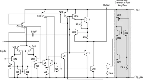
Figure 1. Representative Circuit Diagram
(One−Fourth of Circuit Shown)
Output
Bias Circuitry
Common to Four
Amplifiers
V
CCV
EE/GND
Inputs
Q2
Q3
Q4
Q5
Q26
Q7
Q8
Q6
Q9
Q11
Q10
Q1
2.4 k
Q25
Q22
40 k
Q13
Q14
Q15
Q16
Q19
5.0 pF
Q18
Q17
Q20
Q21
2.0 k
Q24
Q23
Q12
25
+
-CIRCUIT DESCRIPTION
The LM324 series is made using four internally
compensated, two−stage operational amplifiers. The first
stage of each consists of differential input devices Q20 and
Q18 with input buffer transistors Q21 and Q17 and the
differential to single ended converter Q3 and Q4. The first
stage performs not only the first stage gain function but also
performs the level shifting and transconductance reduction
functions. By reducing the transconductance, a smaller
compensation capacitor (only 5.0 pF) can be employed, thus
saving chip area. The transconductance reduction is
accomplished by splitting the collectors of Q20 and Q18.
Another feature of this input stage is that the input common
mode range can include the negative supply or ground, in
single supply operation, without saturating either the input
devices or the differential to single−ended converter. The
second stage consists of a standard current source load
amplifier stage.
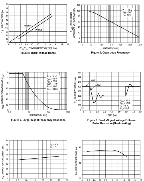
Figure 2. Large Signal Voltage Follower Response
V
CC= 15 Vdc
R
L= 2.0 k
W
T
A= 25
°
C
5.0
m
s/DIV
1.0 V/DIV
Each amplifier is biased from an internal−voltage
regulator which has a low temperature coefficient thus
giving each amplifier good temperature characteristics as
well as excellent power supply rejection.
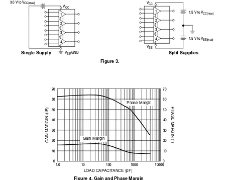
Single Supply
Split Supplies
V
CCV
EE/GND
3.0 V to V
CC(max)1
2
3
4
V
CC1
2
3
4
V
EE1.5 V to V
CC(max)1.5 V to V
EE(max)Figure 3.
70
60
50
40
30
20
10
0
1.0
10
100
10000
LOAD CAPACITANCE (pF)
Phase Margin
Figure 4. Gain and Phase Margin
1000
70
60
50
40
30
20
10
0
GAIN MARGIN (dB)
PHASE MARGIN (
°
)
V
OR
, OUTPUT
VOL
TAGE RANGE (V
)
pp
V
O
, OUTPUT
VOL
TAGE (mV)
14
f, FREQUENCY (kHz)
550
V
CC, POWER SUPPLY VOLTAGE (V)
V
CC, POWER SUPPLY VOLTAGE (V)
90
CURRENT
(mA)
CC
I , INPUT
BIAS CURRENT
(nA)
Figure 5. Input Voltage Range
Figure 6. Open Loop Frequency
120
f, FREQUENCY (Hz)
A
, LARGE-SIGNAL VOL
OPEN LOOP
VOL
TAGE GAIN (dB)
V
CC= 15 V
V
EE= GND
T
A= 25
°
C
Figure 7. Large−Signal Frequency Response
Figure 8. Small−Signal Voltage Follower
Pulse Response (Noninverting)
2
Notch Output
V
ref=
V
CCWhere: T
BP= Center Frequency Gain
Where:
T
N= Passband Notch Gain
R = 160 k
W
LM324
1/4LM324
1/4
LM324
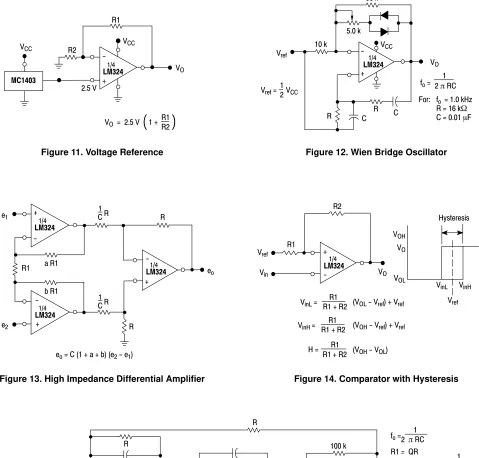
Figure 11. Voltage Reference
Figure 12. Wien Bridge Oscillator
2
1
For less than 10% error from operational amplifier,
If source impedance varies, filter may be preceded with
voltage follower buffer to stabilize filter parameters.
where f
oand BW are expressed in Hz.
Q
of
oBW
< 0.1
Given: f
o= center frequency
A(f
o) = gain at center frequency
Choose value f
o, C
Then:
R3 =
Q
p
f
oC
R3
R1 =
2 A(f
o)
R1 R3
4Q
2R1 - R3
R2 =
+
-+
-V
ref=
V
CCV
reff =
R1 + R
C4 CR
fR1
R3 =
R2 R1
R2 + R1
R2
300 k
75 k
R3
R1
100 k
C
Triangle Wave
Output
Square
Wave
Output
V
inR
fif
V
ref1/4
LM324
1/4
LM324
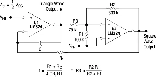
Figure 16. Function Generator
Figure 17. Multiple Feedback Bandpass Filter
V
ref=
1
2
V
CC-+
V
CCR3
R1
R2
V
refC
C
V
OCO = 10 C
C
O1/4
ORDERING INFORMATION
Device
Operating Temperature Range
Package
Shipping
†LM224DG
−25
°
C to +85
°
C
SOIC−14 (Pb−Free)
55 Units/Rail
LM224DR2G
SOIC−14 (Pb−Free)
2500/Tape & Reel
LM224DTBG
TSSOP−14 (Pb−Free)
96 Units/Tube
LM224DTBR2G
TSSOP−14 (Pb−Free)
2500/Tape & Reel
LM224NG
PDIP−14 (Pb−Free)
25 Units/Rail
LM324DG
0
°
C to +70
°
C
SOIC−14 (Pb−Free)
55 Units/Rail
LM324DR2G
SOIC−14 (Pb−Free)
2500/Tape & Reel
LM324EDR2G
SOIC−14 (Pb−Free)
2500/Tape & Reel
LM324DTBG
TSSOP−14 (Pb−Free)
96 Units/Tube
LM324DTBR2G
TSSOP−14 (Pb−Free)
2500/Tape & Reel
LM324NG
PDIP−14 (Pb−Free)
25 Units/Rail
LM324ADG
SOIC−14 (Pb−Free)
55 Units/Rail
LM324ADR2G
SOIC−14 (Pb−Free)
2500/Tape & Reel
LM324ADTBG
TSSOP−14 (Pb−Free)
96 Units/Tube
LM324ADTBR2G
TSSOP−14 (Pb−Free)
2500/Tape & Reel
LM324ANG
PDIP−14 (Pb−Free)
25 Units/Rail
LM2902DG
−40
°
C to +105
°
C
SOIC−14 (Pb−Free)
55 Units/Rail
LM2902DR2G
SOIC−14 (Pb−Free)
2500/Tape & Reel
LM2902EDR2G
SOIC−14 (Pb−Free)
2500/Tape & Reel
LM2902DTBG
TSSOP−14 (Pb−Free)
96 Units/Tube
LM2902DTBR2G
TSSOP−14 (Pb−Free)
2500/Tape & Reel
LM2902NG
PDIP−14 (Pb−Free)
25 Units/Rail
LM2902VDG
−40
°
C to +125
°
C
SOIC−14 (Pb−Free)
55 Units/Rail
LM2902VDR2G
SOIC−14 (Pb−Free)
2500/Tape & Reel
LM2902VDTBG
TSSOP−14 (Pb−Free)
96 Units/Tube
LM2902VDTBR2G
TSSOP−14 (Pb−Free)
2500/Tape & Reel
LM2902VNG
PDIP−14 (Pb−Free)
25 Units/Rail
NCV2902DR2G*
SOIC−14 (Pb−Free)
2500/Tape & Reel
NCV2902DTBR2G*
TSSOP−14 (Pb−Free)
†For information on tape and reel specifications, including part orientation and tape sizes, please refer to our Tape and Reel Packaging
Specifications Brochure, BRD8011/D.
MARKING DIAGRAMS
x
= 2 or 3
A
= Assembly Location
WL, L
= Wafer Lot
YY, Y
= Year
WW, W
= Work Week
G or
G
= Pb−Free Package
PDIP−14
N SUFFIX
CASE 646
SOIC−14
D SUFFIX
CASE 751A
1
14
LM324AN
AWLYYWWG
1
14
LMx24N
AWLYYWWG
1
14
LM2902N
AWLYYWWG
1
14
LM2902VN
AWLYYWWG
*This marking diagram also applies to NCV2902.
TSSOP−14
DTB SUFFIX
CASE 948G
1
14
x24
ALYW
G
G
1
14
1
14
1
14
*
324A
ALYW
G
G
2902
ALYW
G
G
2902
V
ALYW
G
G
LM324ADG
AWLYWW
1
14
LMx24DG
AWLYWW
1
14
LM2902DG
AWLYWW
1
14
LM2902VDG
AWLYWW
1
14
(Note: Microdot may be in either location)
LMx24EG
AWLYWW
1
14
LM2902EG
AWLYWW
1
PACKAGE DIMENSIONS
SOIC−14
CASE 751A−03
ISSUE K
NOTES:
1. DIMENSIONING AND TOLERANCING PER ASME Y14.5M, 1994.
2. CONTROLLING DIMENSION: MILLIMETERS. 3. DIMENSION b DOES NOT INCLUDE DAMBAR
PROTRUSION. ALLOWABLE PROTRUSION SHALL BE 0.13 TOTAL IN EXCESS OF AT MAXIMUM MATERIAL CONDITION. 4. DIMENSIONS D AND E DO NOT INCLUDE
MOLD PROTRUSIONS.
5. MAXIMUM MOLD PROTRUSION 0.15 PER SIDE.
H
14 8
7 1
M
0.25
B
MC
h
X 45SEATING PLANE
A1
A
M
_
S
A
M0.25
C
B
Sb
13XB
A
E
D
e
DETAIL A
L
A3
DETAIL A
DIM MIN MAX MIN MAX INCHES MILLIMETERS
D 8.55 8.75 0.337 0.344 E 3.80 4.00 0.150 0.157 A 1.35 1.75 0.054 0.068 b 0.35 0.49 0.014 0.019
L 0.40 1.25 0.016 0.049 e 1.27 BSC 0.050 BSC A3 0.19 0.25 0.008 0.010 A1 0.10 0.25 0.004 0.010
M 0 7 0 7 H 5.80 6.20 0.228 0.244 h 0.25 0.50 0.010 0.019
_
_
_
_
6.50
14X
0.58
14X
1.18
1.27
DIMENSIONS: MILLIMETERS
1
PITCH
SOLDERING FOOTPRINT*
PACKAGE DIMENSIONS
TSSOP−14
CASE 948G
ISSUE B
DIM MIN MAX MIN MAX INCHES MILLIMETERS
A 4.90 5.10 0.193 0.200 B 4.30 4.50 0.169 0.177 C −−− 1.20 −−− 0.047 D 0.05 0.15 0.002 0.006 F 0.50 0.75 0.020 0.030 G 0.65 BSC 0.026 BSC H 0.50 0.60 0.020 0.024 J 0.09 0.20 0.004 0.008 J1 0.09 0.16 0.004 0.006 K 0.19 0.30 0.007 0.012 K1 0.19 0.25 0.007 0.010 L 6.40 BSC 0.252 BSC M 0 8 0 8 NOTES:
1. DIMENSIONING AND TOLERANCING PER ANSI Y14.5M, 1982.
2. CONTROLLING DIMENSION: MILLIMETER. 3. DIMENSION A DOES NOT INCLUDE MOLD FLASH, PROTRUSIONS OR GATE BURRS. MOLD FLASH OR GATE BURRS SHALL NOT EXCEED 0.15 (0.006) PER SIDE.
4. DIMENSION B DOES NOT INCLUDE INTERLEAD FLASH OR PROTRUSION. INTERLEAD FLASH OR PROTRUSION SHALL NOT EXCEED 0.25 (0.010) PER SIDE. 5. DIMENSION K DOES NOT INCLUDE DAMBAR
PROTRUSION. ALLOWABLE DAMBAR PROTRUSION SHALL BE 0.08 (0.003) TOTAL IN EXCESS OF THE K DIMENSION AT MAXIMUM MATERIAL CONDITION. 6. TERMINAL NUMBERS ARE SHOWN FOR
REFERENCE ONLY.
7. DIMENSION A AND B ARE TO BE DETERMINED AT DATUM PLANE −W−.
_
_
_
_
0.10 (0.004)
−T−
ÇÇÇ
ÇÇÇ
SECTION N−N
DETAIL E
J J1
K
K1
ÉÉÉ
ÉÉÉ
DETAIL E
F
M
−W−
0.25 (0.010)
80.36
14X1.26
0.65
DIMENSIONS: MILLIMETERS
1
PITCH
PACKAGE DIMENSIONS
PDIP−14
CASE 646−06
ISSUE S
1 7
14 8
b2
NOTE 8D
A
TOP VIEW
E1
SIDE VIEW
M14X
END VIEW
END VIEW
WITH LEADS CONSTRAINEDDIM MIN MAX INCHES
A −−−− 0.210 A1 0.015 −−−− b 0.014 0.022 C 0.008 0.014 D 0.735 0.775 D1 0.005 −−−− e 0.100 BSC E 0.300 0.325
M −−−− 10
−−− 5.33 0.38 −−− 0.35 0.56 0.20 0.36 18.67 19.69 0.13 −−−
2.54 BSC 7.62 8.26
−−− 10 MIN MAX MILLIMETERS NOTES:
1. DIMENSIONING AND TOLERANCING PER ASME Y14.5M, 1994. 2. CONTROLLING DIMENSION: INCHES.
3. DIMENSIONS A, A1 AND L ARE MEASURED WITH THE PACK-AGE SEATED IN JEDEC SEATING PLANE GAUGE GS−3. 4. DIMENSIONS D, D1 AND E1 DO NOT INCLUDE MOLD FLASH
OR PROTRUSIONS. MOLD FLASH OR PROTRUSIONS ARE NOT TO EXCEED 0.10 INCH.
5. DIMENSION E IS MEASURED AT A POINT 0.015 BELOW DATUM PLANE H WITH THE LEADS CONSTRAINED PERPENDICULAR TO DATUM C.
6. DIMENSION eB IS MEASURED AT THE LEAD TIPS WITH THE LEADS UNCONSTRAINED.
7. DATUM PLANE H IS COINCIDENT WITH THE BOTTOM OF THE LEADS, WHERE THE LEADS EXIT THE BODY.
8. PACKAGE CONTOUR IS OPTIONAL (ROUNDED OR SQUARE CORNERS).
E1 0.240 0.280 6.10 7.11 b2
eB −−−− 0.430 −−− 10.92 0.060 TYP 1.52 TYP
c
A2 0.115 0.195 2.92 4.95
L 0.115 0.150 2.92 3.81
°