programmable logic devices 1
PROGRAMMABLE LOGIC DEVICES
“ Hardware make softer, software make harder “
•Perkembangan Teknologi Logic Device
•Definisi PLD
•Konsep Dasar PLD
•Jenis-jenis PLD : PAL, PLA, GAL
•Memprogram dan men-develop pogram PLD
•Jenis PLD yang lain : FPLA, FPGA, CPLD
programmable logic devices 2 Source: Dataquest Logic Standard Logic ASIC Programmable Logic Devices (PLDs) Gate Arrays Cell-Based ICs Full Custom ICs CPLDs SPLDs (PALs) FPGAs
Perkembangan Teknologi Logic Devices
Acronyms
SPLD = Simple Programmable Logic Device PAL = Programmable Array of Logic
CPLD = Complex PLD
FPGA = Field Programmable Gate Array
programmable logic devices 3
PLD Æ sebuah IC yang terdiri dari banyak gate / gerbang
logika (terdiri dari gerbang AND, OR, NOT, register
dan flip-flop), yang saling diinterkoneksikan di dalam
IC tersebut.
Definisi
Programmable Æ untuk membuat sebuah fungsi pada PLD
tersebut, seorang disainer harus membuat
program yang nantinya akan menyebabkan
terjadinya proses “fuse blowing” pada
interkoneksi gerbang, flip-flop maupun register,
sehingga didapatkan pola rangkaian seperti yang
diinginkan.
programmable logic devices 4
Konsep Dasar
A A A B B B AB AB AB AB Input linesSum of Product Output
Product lines
OR array AND array
programmable logic devices 5 1 9 3 4 5 6 7 8 2 10 11 12 13 14 15 16 A B C D AND array (hard wired) 0 1 2 3 O3O2O1O0 OR array (programmable) OUTPUT x x x x x x x x x x x x x x x x x x x x x x x x x x x x x x x x x x x x x x x x x x x x x x x x x x x x x x x x x x x x x x x x Fuse tersedia Arsitektur PROM untuk PLD
Contoh :
AM27S13
-PROM dengan konfigurasi 512x4
-Ada 512 address
-Dengan 9 jalur address input
-Ada 4 data output
programmable logic devices 6
Fuse “blown” untuk mendapatkan output sesuai fungsi yang diinginkan
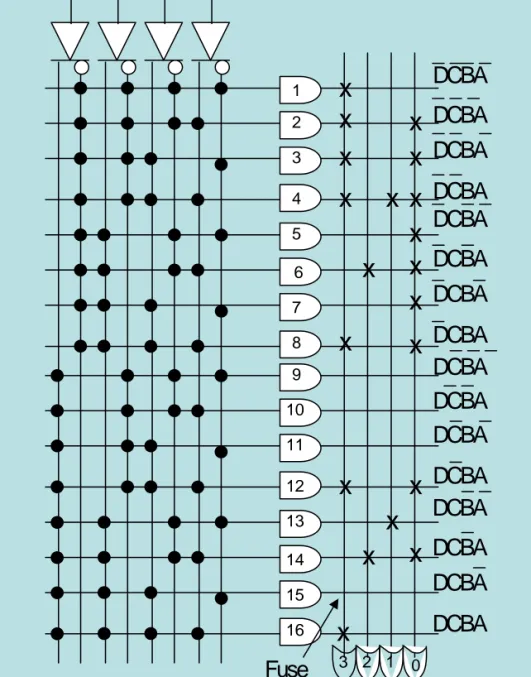
O3 = AB + CD O2 = ABC O1 = ABCD + ABCD O0 = A + BD + CD 1 9 3 4 5 6 7 8 2 10 11 12 13 14 15 16 A B C D 0 1 2 3 O3O2O1O0 Fuse “blown” x x x x x x x x x x x x x x x x x x x x DCBA DCBA DCBA DCBA DCBA DCBA DCBA DCBA DCBA DCBA DCBA DCBA DCBA DCBA DCBA DCBA D C B A O3 0 0 0 0 1 0 0 0 1 1 0 0 1 0 1 0 0 1 1 1 0 1 0 0 0 0 1 0 1 0 0 1 1 0 0 0 1 1 1 1 1 0 0 0 0 1 0 0 1 0 1 0 1 0 0 1 0 1 1 1 1 1 0 0 0 1 1 0 1 0 1 1 1 0 0 1 1 1 1 1 DCBA DCBA DCBA DCBA DCBA DCBA DCBA
programmable logic devices 7 1 9 3 4 5 6 7 8 2 10 11 12 13 14 15 16 x x x x x x x x x x x x x x x x x x x x x x x x x x x x x x x x x x x x x x x x x x x x x x x x x x x x x x x x x x x x x x x x x x x x x x x x x x x x x x x x x x x x x x x x x x x x x x x x x x x x x x x x x x x x x x x x x x x x x x x x x x x x x x x x A B C D AND array (programmable) 0 1 2 3 O3 O2O1O0 OR array (hard wired) OUTPUT
Programmable Array Logic (PAL)
Arsitektur mirip dengan PROM,
di bagian AND array adalah programmable,
sedangkan di bagian OR array adalah hard wired Kelebihan dibandingkan dengan PROM,
hanya fungsi AND yang diinginkan saja yang diprogram, dan output masing-masing AND disambungkan
ke array OR
Output OR merupakan fungsi jumlahan dari fungsi-fungsi AND yang diinginkan
programmable logic devices 8 1 9 3 4 5 6 7 8 2 10 11 12 13 14 15 16 A B C D 0 1 2 3 O3 O2O1O0 x x x x x x x x x x x x x x x x x x x x x x x x x x x x x x x x x x x x x x x x x x x x x x x x x x x x x x x x x x x x x x x x x x x x x x x x x x x x x x x x x x x x AB CD 0 0 ABC 0 0 0 ABCD ABCD A BD CD 0 0 0 PAL diprogram sesuai fungsi yang diinginkan
• Setiap OR maksimum hanya dapat menjumlahkan 4 buah minterm (dengan konfigurasi di samping). • Jika sebuah OR hanya terisi kurang dari 4 minterm,
maka minterm / AND array yang tidak digunakan diberi nilai “0”
O3 = AB + CD + 0 + 0 = AB + CD O2 = ABC + 0 + 0 + 0 = ABC
O1 = ABCD + ABCD
programmable logic devices 9
Field Programmable Logic Array (FPLA)
Lebih kompleks dari PAL.
Juga terdiri dari array programmable input AND dan array output OR. Mempunyai fleksibilitas untuk memprogram input OR
Complex Programmable Logic Devices (CPLD)
Merupakan PLD dalam kapasitas lebih besar. Terdiri dari beberapa PLD (multiple PLD)
programmable logic devices 10
Field Programmable Gate Array (FPGA)
• Dikonfigurasi oleh End User
• Tidak memerlukan proses Fabrikasi
• Tersedia solusi yang mendukung chip customized VLSI
• Mampu menimplementasikan logic circuit, instant manufacturring, very-low cost prototype
• Pemrograman yang singkat untuk fungsi dan kemampuan yang setara dengan ASIC
programmable logic devices 11 CLB CLB CLB CLB Switch Matrix Programmable
Interconnect I/O Blocks (IOBs)
Configurable Logic Blocks (CLBs) D Q Slew Rate Control Passive Pull-Up, Pull-Down Delay Vcc Output Buffer Input Buffer Q D Pad D Q SD RD EC S/R Control D Q SD RD EC S/R Control 1 1 F' G' H' DIN F' G' H' DIN F' G' H' H' H Func. Gen. G Func. Gen. F Func. Gen. G4 G3 G2 G1 F4 F3 F2 F1 C4 C1 C2 C3 K Y X H1 DIN S/R EC
programmable logic devices 12 Memprogram PLD
Flow Chart Mendisain, Memprogram dan mengetes PLD
START Develop circuit logic equation Run program development software Input logic equation Software generate fuse map
and test data
Send fuse map and test data to programmer Program the PLD Test the PLD Works ? Test the PLD in its actual circuit Check design equations Works ? Troubleshoot DONE Y Y N N A A
programmable logic devices 13 Beberapa peralatan yang diperlukan untuk mendisain dan
membangun rangkaian menggunakan PLD : •Personal Computer (PC)
•PLD Development Software •Programming fixture
•Software untuk men-drive programming fixture •Programmable Logic Device
Programming Software PLD Development Software PC Programming Fixture
Serial Cable ZIF Socket
programmable logic devices 14
Programmable Logic - Design Flow
XC4000 XC4000
XC4000
3
Design Entry dengan cara schematic, ABEL, VHDL,
dan/atau Verilog.
Implementation yaitu Placement & Routing dan
bitstream generation. Juga, analyze timing, view layout, .
Download meng-upload bitstream ke
Hardware (FPGA chip)
1
programmable logic devices 15
programmable logic devices 16
Flowchart siklus developing PLD
Troubleshoot
Create JEDEC file Program PLD In-circuit test Works ? DONE Identify design flaw
Edit source file
Design
Create source file Compile Errors? Simulate Problems? Y Y Y N N N
programmable logic devices 17
Verilog HDL / VHDL
– Verilog HDL / VHDL adalah Bahasa
Pendeskripsi Perangkat Keras / Hardware
Description Language (HDL).
– Hardware Description Language adalah
bahasa yang dapat digunakan untuk
mendeskripsikan sebuah sistim digital, misal,
sebuah komputer atau komponen dari
programmable logic devices 18
Apakah Verilog HDL / VHDL?
• Verilog adalah salah satu HDL yang digunakan
oleh disainer hardware dalam industri maupun
sekolah.
• HDL yang lain adalah VHDL (Very High-speed
Integrated Circuit HDL)
• VHDL dibuat dengan standart IEEE pada tahun
1987, sedangkan Verilog pada tahun 1995.
• Verilog sangat menyerupai C, dan para insinyur
elektronika dan komputer sudah familiar dengan
bahasa C.
• VHDL menyerupai
EDA (Electronic Digital
programmable logic devices 19
• Entity dan Architecture
• Modeling: Behavior ,
Structure dan data Flow
Struktur Pemrograman VHDL
programmable logic devices 20
Ada tiga cara untuk
mendiskripsikan Rangkaian
1. Structural
–
Didesain berdasarkan perkomponen dan
“merangkai komponen tersebut
2. Dataflow (RTL)
–
Didesain berdasarkan alur register data
3. Behavioural
programmable logic devices 21
• Entity Declaration
– Spesifikasi eksternal dari rangkaian
• Architecture Body
– Fungsi sesungguhnya dari rangkaian
• Disain deskripsi minimum VHDL terdiri dari :
– Paling sedikit satu entity dan satu Architecture
Body
Architecture Body
programmable logic devices 22
Entity
Konstruksi “Entity” berfungsi memodelkan interface eksternal
d3
d2
d1
d0
q0
q1
q2
q3
en
clk
Internal
Functionality
REG_4
External
External
Interface
Interface
programmable logic devices 23
entity reg4 is
port (do,d1,d2,d3,en,clk : in bit;
qo,q1,q3,q4: out bit;);
end entity reg4;
“port” VHDL membentuk model data input/output.
Entity name
Port name
Port
Port mode
ENTITY entity-name IS
[PORT(interface-signal-declaration);] END [ENTITY] [entity-name];
programmable logic devices 24 ENTITY compare IS
PORT(a, b: IN bit_vector(0 TO 7);
eq: OUT bit);
END compare; A[8] B[8] EQ 8-bit Comparator Rangkaian 1 (8-bit Comparator)
programmable logic devices 25
Architecture Body
• Fungsi sesungguhnya dari circuit
ARCHITECTURE arch-name OF entity-name IS [declarations]
BEGIN
architecture body
programmable logic devices 26 Architecture body dari rangkaian 1 adalah :
ARCHITECTURE compare1 OF compare IS BEGIN
eq <= ‘1’ WHEN (a=b) ELSE ‘0’; END compare1;
programmable logic devices 27 HDL total dari rangkaian 1 adalah :
ENTITY compare IS
PORT(a, b: IN bit_vector(0 TO 7); eq: OUT bit);
END compare;
ARCHITECTURE compare1 OF compare IS BEGIN
eq <= ‘1’ WHEN (a=b) ELSE ‘0’; END compare1;
programmable logic devices 28 Rangkaian 2 (Full Adder)
ENTITY fulladder IS
PORT(x, y, cin: IN bit; cout, sum: OUT bit); END fulladder;
ARCHITECTURE concurrent OF fulladder IS BEGIN
sum <= x XOR y XOR cin;
cout <= (x AND y) OR (x AND cin) OR (y AND cin); END concurrent; cout sum y x cin
programmable logic devices 29
Behavioral Description
LIBRARY ieee;
USE ieee.std_logic_1164.ALL ENTITY eqcomp4 IS PORT(
a, b: IN std_logic_vector(3 DOWNTO 0); equals: OUT std_logic);
END eqcomp4;
ARCHITECTURE behavioral OF eqcomp4 IS BEGIN
comp: PROCESS (a, b) BEGIN IF a = b then equals <= ‘1’; ELSE equals <= ‘0’; END IF;
END PROCESS comp; END behavioral;
programmable logic devices 30
Dataflow(RTL) Description
LIBRARY ieee;
USE ieee.std_logic_1164.ALL
ENTITY eqcomp4 IS PORT(
a, b: IN std_logic_vector(3 DOWNTO 0);
equals: OUT std_logic);
END eqcomp4;
ARCHITETURE dataflow OF eqcomp4 IS
BEGIN
equals <= ‘1’ WHEN (a=b) ELSE ‘0’;
END dataflow;
programmable logic devices 31