• 4K Bytes of In-System Programmable (ISP) Flash Memory – Endurance: 1000 Write/Erase Cycles
• 4.0V to 5.5V Operating Range
• Fully Static Operation: 0 Hz to 33 MHz • Three-level Program Memory Lock • 128 x 8-bit Internal RAM
• 32 Programmable I/O Lines • Two 16-bit Timer/Counters • Six Interrupt Sources
• Full Duplex UART Serial Channel • Low-power Idle and Power-down Modes • Interrupt Recovery from Power-down Mode • Watchdog Timer
• Dual Data Pointer • Power-off Flag
• Fast Programming Time
• Flexible ISP Programming (Byte and Page Mode) • Green (Pb/Halide-free) Packaging Option
1.
Description
The AT89S51 is a low-power, high-performance CMOS 8-bit microcontroller with 4K bytes of In-System Programmable Flash memory. The device is manufactured using Atmel’s high-density nonvolatile memory technology and is compatible with the indus-try-standard 80C51 instruction set and pinout. The on-chip Flash allows the program memory to be reprogrammed in-system or by a conventional nonvolatile memory pro-grammer. By combining a versatile 8-bit CPU with In-System Programmable Flash on a monolithic chip, the Atmel AT89S51 is a powerful microcontroller which provides a highly-flexible and cost-effective solution to many embedded control applications. The AT89S51 provides the following standard features: 4K bytes of Flash, 128 bytes of RAM, 32 I/O lines, Watchdog timer, two data pointers, two 16-bit timer/counters, a five-vector two-level interrupt architecture, a full duplex serial port, on-chip oscillator, and clock circuitry. In addition, the AT89S51 is designed with static logic for operation down to zero frequency and supports two software selectable power saving modes. The Idle Mode stops the CPU while allowing the RAM, timer/counters, serial port, and interrupt system to continue functioning. The Power-down mode saves the RAM con-tents but freezes the oscillator, disabling all other chip functions until the next external interrupt or hardware reset.
8-bit
Microcontroller
with 4K Bytes
In-System
Programmable
Flash
AT89S51
2.
Pin Configurations
2.1
40-lead PDIP
2.2
44-lead TQFP
1 2 3 4 5 6 7 8 9 10 11 12 13 14 15 16 17 18 19 20 40 39 38 37 36 35 34 33 32 31 30 29 28 27 26 25 24 23 22 21 P1.0 P1.1 P1.2 P1.3 P1.4 (MOSI) P1.5 (MISO) P1.6 (SCK) P1.7 RST (RXD) P3.0 (TXD) P3.1 (INT0) P3.2 (INT1) P3.3 (T0) P3.4 (T1) P3.5 (WR) P3.6 (RD) P3.7 XTAL2 XTAL1 GND VCC P0.0 (AD0) P0.1 (AD1) P0.2 (AD2) P0.3 (AD3) P0.4 (AD4) P0.5 (AD5) P0.6 (AD6) P0.7 (AD7) EA/VPP ALE/PROG PSEN P2.7 (A15) P2.6 (A14) P2.5 (A13) P2.4 (A12) P2.3 (A11) P2.2 (A10) P2.1 (A9) P2.0 (A8) 1 2 3 4 5 6 7 8 9 10 11 33 32 31 30 29 28 27 26 25 24 23
44 43 42 41 40 39 38 37 36 35 34
12 13 14 15 16 17 18 19 20 21 22
(MOSI) P1.5 (MISO) P1.6 (SCK) P1.7 RST (RXD) P3.0 NC (TXD) P3.1 (INT0) P3.2 (INT1) P3.3 (T0) P3.4 (T1) P3.5 P0.4 (AD4) P0.5 (AD5) P0.6 (AD6) P0.7 (AD7) EA/VPP NC ALE/PROG PSEN P2.7 (A15) P2.6 (A14) P2.5 (A13)
P1.4 P1.3 P1.2 P1.1 P1.0 NC VCC P0.0 (AD0) P0.1 (AD1) P0.2 (AD2) P0.3 (AD3)
(WR) P3.6 (RD) P3.7 XTAL2 XTAL1 GND GND
(A8) P2.0 (A9) P2.1 (A10) P2.2 (A11) P2.3 (A12) P2.4
2.3
44-lead PLCC
2.4
42-lead PDIP
7 8 9 10 11 12 13 14 15 16 17 39 38 37 36 35 34 33 32 31 30 29 (MOSI) P1.5 (MISO) P1.6 (SCK) P1.7 RST (RXD) P3.0 NC (TXD) P3.1 (INT0) P3.2 (INT1) P3.3 (T0) P3.4 (T1) P3.5 P0.4 (AD4) P0.5 (AD5) P0.6 (AD6) P0.7 (AD7) EA/VPP NC ALE/PROG PSEN P2.7 (A15) P2.6 (A14) P2.5 (A13) 6 5 4 3 2 1 44 43 42 41 40
18 19 20 21 22 23 24 25 26 27 28
(WR) P3.6 (RD) P3.7 XTAL2 XTAL1 GND
NC
(A8) P2.0 (A9) P2.1 (A10) P2.2 (A11) P2.3 (A12) P2.4 P1.4 P1.3 P1.2 P1.1 P1.0 NC VCC P0.0 (AD0) P0.1 (AD1) P0.2 (AD2) P0.3 (AD3)
3.
Block Diagram
PORT 2 DRIVERS
PORT 2 LATCH
P2.0 - P2.7
FLASH PORT 0
LATCH RAM
PROGRAM ADDRESS REGISTER
BUFFER
PC INCREMENTER
PROGRAM COUNTER
DUAL DPTR INSTRUCTION
REGISTER B
REGISTER
INTERRUPT, SERIAL PORT, AND TIMER BLOCKS
STACK POINTER ACC
TMP2 TMP1
ALU
PSW
TIMING AND CONTROL
PORT 1 DRIVERS
P1.0 - P1.7 PORT 3
LATCH
PORT 3 DRIVERS
P3.0 - P3.7 OSC
GND
VCC
PSEN
ALE/PROG
EA / VPP
RST
RAM ADDR. REGISTER
PORT 0 DRIVERS P0.0 - P0.7
PORT 1 LATCH WATCH
4.
Pin Description
4.1
VCC
Supply voltage (all packages except 42-PDIP).
4.2
GND
Ground (all packages except 42-PDIP; for 42-PDIP GND connects only the logic core and the embedded program memory).
4.3
VDD
Supply voltage for the 42-PDIP which connects only the logic core and the embedded program memory.
4.4
PWRVDD
Supply voltage for the 42-PDIP which connects only the I/O Pad Drivers. The application board
MUST connect both VDD and PWRVDD to the board supply voltage.
4.5
PWRGND
Ground for the 42-PDIP which connects only the I/O Pad Drivers. PWRGND and GND are weakly connected through the common silicon substrate, but not through any metal link. The application board MUST connect both GND and PWRGND to the board ground.
4.6
Port 0
Port 0 is an 8-bit open drain bi-directional I/O port. As an output port, each pin can sink eight TTL inputs. When 1s are written to port 0 pins, the pins can be used as high-impedance inputs. Port 0 can also be configured to be the multiplexed low-order address/data bus during accesses to external program and data memory. In this mode, P0 has internal pull-ups.
Port 0 also receives the code bytes during Flash programming and outputs the code bytes dur-ing program verification. External pull-ups are required during program verification.
4.7
Port 1
Port 1 is an 8-bit bi-directional I/O port with internal pull-ups. The Port 1 output buffers can sink/source four TTL inputs. When 1s are written to Port 1 pins, they are pulled high by the inter-nal pull-ups and can be used as inputs. As inputs, Port 1 pins that are exterinter-nally being pulled low will source current (IIL) because of the internal pull-ups.
Port 1 also receives the low-order address bytes during Flash programming and verification.
Port Pin Alternate Functions
P1.5 MOSI (used for In-System Programming)
4.8
Port 2
Port 2 is an 8-bit bi-directional I/O port with internal pull-ups. The Port 2 output buffers can sink/source four TTL inputs. When 1s are written to Port 2 pins, they are pulled high by the inter-nal pull-ups and can be used as inputs. As inputs, Port 2 pins that are exterinter-nally being pulled low will source current (IIL) because of the internal pull-ups.
Port 2 emits the high-order address byte during fetches from external program memory and dur-ing accesses to external data memory that use 16-bit addresses (MOVX @ DPTR). In this application, Port 2 uses strong internal pull-ups when emitting 1s. During accesses to external data memory that use 8-bit addresses (MOVX @ RI), Port 2 emits the contents of the P2 Special Function Register.
Port 2 also receives the high-order address bits and some control signals during Flash program-ming and verification.
4.9
Port 3
Port 3 is an 8-bit bi-directional I/O port with internal pull-ups. The Port 3 output buffers can sink/source four TTL inputs. When 1s are written to Port 3 pins, they are pulled high by the inter-nal pull-ups and can be used as inputs. As inputs, Port 3 pins that are exterinter-nally being pulled low will source current (IIL) because of the pull-ups.
Port 3 receives some control signals for Flash programming and verification.
Port 3 also serves the functions of various special features of the AT89S51, as shown in the fol-lowing table.
4.10
RST
Reset input. A high on this pin for two machine cycles while the oscillator is running resets the device. This pin drives High for 98 oscillator periods after the Watchdog times out. The DIS-RTO bit in SFR AUXR (address 8EH) can be used to disable this feature. In the default state of bit DISRTO, the RESET HIGH out feature is enabled.
4.11
ALE/PROG
Address Latch Enable (ALE) is an output pulse for latching the low byte of the address during accesses to external memory. This pin is also the program pulse input (PROG) during Flash programming.
Port Pin Alternate Functions
P3.0 RXD (serial input port)
P3.1 TXD (serial output port)
P3.2 INT0 (external interrupt 0)
P3.3 INT1 (external interrupt 1)
P3.4 T0 (timer 0 external input)
P3.5 T1 (timer 1 external input)
P3.6 WR (external data memory write strobe)
In normal operation, ALE is emitted at a constant rate of 1/6 the oscillator frequency and may be used for external timing or clocking purposes. Note, however, that one ALE pulse is skipped dur-ing each access to external data memory.
If desired, ALE operation can be disabled by setting bit 0 of SFR location 8EH. With the bit set, ALE is active only during a MOVX or MOVC instruction. Otherwise, the pin is weakly pulled high. Setting the ALE-disable bit has no effect if the microcontroller is in external execution mode.
4.12
PSEN
Program Store Enable (PSEN) is the read strobe to external program memory.
When the AT89S51 is executing code from external program memory, PSEN is activated twice each machine cycle, except that two PSEN activations are skipped during each access to exter-nal data memory.
4.13
EA/VPP
External Access Enable. EA must be strapped to GND in order to enable the device to fetch code from external program memory locations starting at 0000H up to FFFFH. Note, however, that if lock bit 1 is programmed, EA will be internally latched on reset.
EA should be strapped to VCC for internal program executions.
This pin also receives the 12-volt programming enable voltage (VPP) during Flash programming.
4.14
XTAL1
Input to the inverting oscillator amplifier and input to the internal clock operating circuit.
4.15
XTAL2
Output from the inverting oscillator amplifier
5.
Special Function Registers
A map of the on-chip memory area called the Special Function Register (SFR) space is shown in
Table 5-1.
User software should not write 1s to these unlisted locations, since they may be used in future products to invoke new fea-tures. In that case, the reset or inactive values of the new bits will always be 0.
Interrupt Registers: The individual interrupt enable bits are in the IE register. Two priorities can be set for each of the five interrupt sources in the IP register.
Table 5-1. AT89S51 SFR Map and Reset Values
0F8H 0FFH
0F0H B
00000000 0F7H
0E8H 0EFH
0E0H ACC
00000000 0E7H
0D8H 0DFH
0D0H PSW
00000000 0D7H
0C8H 0CFH
0C0H 0C7H
0B8H IP
XX000000 0BFH
0B0H P3
11111111 0B7H
0A8H IE
0X000000 0AFH
0A0H P2
11111111
AUXR1 XXXXXXX0
WDTRST
XXXXXXXX 0A7H
98H SCON
00000000
SBUF
XXXXXXXX 9FH
90H P1
11111111 97H
88H TCON
00000000
TMOD 00000000
TL0 00000000
TL1 00000000
TH0 00000000
TH1 00000000
AUXR
XXX00XX0 8FH
80H P0
11111111
SP 00000111
DP0L 00000000
DP0H 00000000
DP1L 00000000
DP1H 00000000
PCON
Dual Data Pointer Registers: To facilitate accessing both internal and external data memory, two banks of 16-bit Data Pointer Registers are provided: DP0 at SFR address locations 82H-83H and DP1 at 84H-85H. Bit DPS = 0 in SFR AUXR1 selects DP0 and DPS = 1 selects DP1. The user should ALWAYS initialize the DPS bit to the appropriate value before accessing the respective Data Pointer Register.
Power Off Flag: The Power Off Flag (POF) is located at bit 4 (PCON.4) in the PCON SFR. POF is set to “1” during power up. It can be set and rest under software control and is not affected by reset.
Table 5-2. AUXR: Auxiliary Register
AUXR Address = 8EH Reset Value = XXX00XX0B
Not Bit Addressable
– – – WDIDLE DISRTO – – DISALE
Bit 7 6 5 4 3 2 1 0
– Reserved for future expansion
DISALE Disable/Enable ALE
DISALE Operating Mode
0 ALE is emitted at a constant rate of 1/6 the oscillator frequency
1 ALE is active only during a MOVX or MOVC instruction
DISRTO Disable/Enable Reset-out
DISRTO
0 Reset pin is driven High after WDT times out
1 Reset pin is input only
WDIDLE Disable/Enable WDT in IDLE mode
WDIDLE
0 WDT continues to count in IDLE mode
6.
Memory Organization
MCS-51 devices have a separate address space for Program and Data Memory. Up to 64K bytes each of external Program and Data Memory can be addressed.
6.1
Program Memory
If the EA pin is connected to GND, all program fetches are directed to external memory.
On the AT89S51, if EA is connected to VCC, program fetches to addresses 0000H through FFFH are directed to internal memory and fetches to addresses 1000H through FFFFH are directed to external memory.
6.2
Data Memory
The AT89S51 implements 128 bytes of on-chip RAM. The 128 bytes are accessible via direct and indirect addressing modes. Stack operations are examples of indirect addressing, so the 128 bytes of data RAM are available as stack space.
7.
Watchdog Timer (One-time Enabled with Reset-out)
The WDT is intended as a recovery method in situations where the CPU may be subjected to software upsets. The WDT consists of a 14-bit counter and the Watchdog Timer Reset (WDTRST) SFR. The WDT is defaulted to disable from exiting reset. To enable the WDT, a user must write 01EH and 0E1H in sequence to the WDTRST register (SFR location 0A6H). When the WDT is enabled, it will increment every machine cycle while the oscillator is running. The WDT timeout period is dependent on the external clock frequency. There is no way to disable the WDT except through reset (either hardware reset or WDT overflow reset). When WDT over-flows, it will drive an output RESET HIGH pulse at the RST pin.
7.1
Using the WDT
To enable the WDT, a user must write 01EH and 0E1H in sequence to the WDTRST register (SFR location 0A6H). When the WDT is enabled, the user needs to service it by writing 01EH and 0E1H to WDTRST to avoid a WDT overflow. The 14-bit counter overflows when it reaches 16383 (3FFFH), and this will reset the device. When the WDT is enabled, it will increment every machine cycle while the oscillator is running. This means the user must reset the WDT at least
Table 5-3. AUXR1: Auxiliary Register 1
AUXR1 Address = A2H Reset Value = XXXXXXX0B
Not Bit Addressable
– – – – – – – DPS
Bit 7 6 5 4 3 2 1 0
– Reserved for future expansion
DPS Data Pointer Register Select
DPS
0 Selects DPTR Registers DP0L, DP0H
every 16383 machine cycles. To reset the WDT the user must write 01EH and 0E1H to WDTRST. WDTRST is a write-only register. The WDT counter cannot be read or written. When WDT overflows, it will generate an output RESET pulse at the RST pin. The RESET pulse dura-tion is 98xTOSC, where TOSC = 1/FOSC. To make the best use of the WDT, it should be serviced in those sections of code that will periodically be executed within the time required to prevent a WDT reset.
7.2
WDT During Power-down and Idle
In down mode the oscillator stops, which means the WDT also stops. While in Power-down mode, the user does not need to service the WDT. There are two methods of exiting Power-down mode: by a hardware reset or via a level-activated external interrupt, which is enabled prior to entering Power-down mode. When Power-down is exited with hardware reset, servicing the WDT should occur as it normally does whenever the AT89S51 is reset. Exiting Power-down with an interrupt is significantly different. The interrupt is held low long enough for the oscillator to stabilize. When the interrupt is brought high, the interrupt is serviced. To prevent the WDT from resetting the device while the interrupt pin is held low, the WDT is not started until the interrupt is pulled high. It is suggested that the WDT be reset during the interrupt service for the interrupt used to exit Power-down mode.
To ensure that the WDT does not overflow within a few states of exiting Power-down, it is best to reset the WDT just before entering Power-down mode.
Before going into the IDLE mode, the WDIDLE bit in SFR AUXR is used to determine whether the WDT continues to count if enabled. The WDT keeps counting during IDLE (WDIDLE bit = 0) as the default state. To prevent the WDT from resetting the AT89S51 while in IDLE mode, the user should always set up a timer that will periodically exit IDLE, service the WDT, and reenter IDLE mode.
With WDIDLE bit enabled, the WDT will stop to count in IDLE mode and resumes the count upon exit from IDLE.
8.
UART
The UART in the AT89S51 operates the same way as the UART in the AT89C51. For further information on the UART operation, please click on the document link below:
http://www.atmel.com/dyn/resources/prod_documents/DOC4316.PDF
9.
Timer 0 and 1
Timer 0 and Timer 1 in the AT89S51 operate the same way as Timer 0 and Timer 1 in the AT89C51. For further information on the timers’ operation, please click on the document link below:
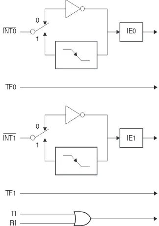
10. Interrupts
The AT89S51 has a total of five interrupt vectors: two external interrupts (INT0 and INT1), two timer interrupts (Timers 0 and 1), and the serial port interrupt. These interrupts are all shown in
Figure 10-1.
Each of these interrupt sources can be individually enabled or disabled by setting or clearing a bit in Special Function Register IE. IE also contains a global disable bit, EA, which disables all interrupts at once.
Note that Table 10-1 shows that bit positions IE.6 and IE.5 are unimplemented. User software should not write 1s to these bit positions, since they may be used in future AT89 products. The Timer 0 and Timer 1 flags, TF0 and TF1, are set at S5P2 of the cycle in which the timers overflow. The values are then polled by the circuitry in the next cycle.
Table 10-1. Interrupt Enable (IE) Register
(MSB) (LSB)
EA – – ES ET1 EX1 ET0 EX0
Enable Bit = 1 enables the interrupt.
Enable Bit = 0 disables the interrupt.
Symbol Position Function
EA IE.7
Disables all interrupts. If EA = 0, no interrupt is acknowledged. If EA = 1, each interrupt source is individually enabled or disabled by setting or clearing its enable bit.
– IE.6 Reserved
– IE.5 Reserved
ES IE.4 Serial Port interrupt enable bit
ET1 IE.3 Timer 1 interrupt enable bit
EX1 IE.2 External interrupt 1 enable bit
ET0 IE.1 Timer 0 interrupt enable bit
EX0 IE.0 External interrupt 0 enable bit
Figure 10-1. Interrupt Sources
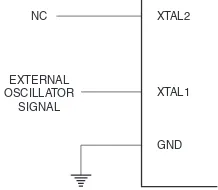
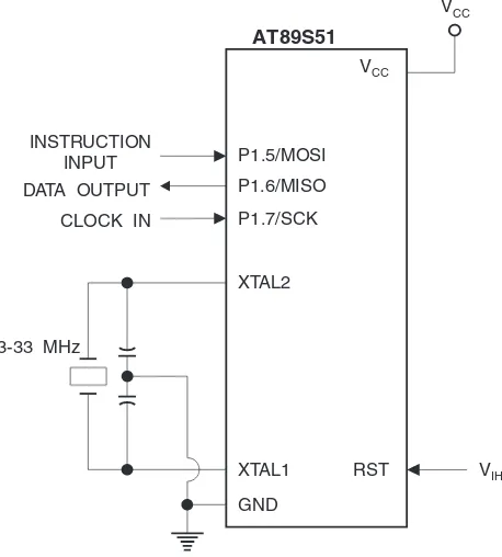
11. Oscillator Characteristics
XTAL1 and XTAL2 are the input and output, respectively, of an inverting amplifier that can be configured for use as an on-chip oscillator, as shown in Figure 11-1. Either a quartz crystal or ceramic resonator may be used. To drive the device from an external clock source, XTAL2 should be left unconnected while XTAL1 is driven, as shown in Figure 11-2. There are no requirements on the duty cycle of the external clock signal, since the input to the internal clock-ing circuitry is through a divide-by-two flip-flop, but minimum and maximum voltage high and low time specifications must be observed.
Figure 11-1. Oscillator Connections
Note: C1, C2 = 30 pF ± 10 pF for Crystals
= 40 pF ± 10 pF for Ceramic Resonators IE1 IE0
1 1
0 0
TF1 TF0
INT1 INT0
TI RI
C2
XTAL2
Figure 11-2. External Clock Drive Configuration
12. Idle Mode
In idle mode, the CPU puts itself to sleep while all the on-chip peripherals remain active. The mode is invoked by software. The content of the on-chip RAM and all the special function regis-ters remain unchanged during this mode. The idle mode can be terminated by any enabled interrupt or by a hardware reset.
Note that when idle mode is terminated by a hardware reset, the device normally resumes pro-gram execution from where it left off, up to two machine cycles before the internal reset algorithm takes control. On-chip hardware inhibits access to internal RAM in this event, but access to the port pins is not inhibited. To eliminate the possibility of an unexpected write to a port pin when idle mode is terminated by a reset, the instruction following the one that invokes idle mode should not write to a port pin or to external memory.
13. Power-down Mode
In the Power-down mode, the oscillator is stopped, and the instruction that invokes Power-down is the last instruction executed. The on-chip RAM and Special Function Registers retain their values until the Power-down mode is terminated. Exit from Power-down mode can be initiated either by a hardware reset or by activation of an enabled external interrupt (INT0 or INT1). Reset redefines the SFRs but does not change the on-chip RAM. The reset should not be activated before VCC is restored to its normal operating level and must be held active long enough to allow the oscillator to restart and stabilize.
XTAL2
XTAL1
GND NC
EXTERNAL OSCILLATOR
SIGNAL
Table 13-1. Status of External Pins During Idle and Power-down Modes
Mode Program Memory ALE PSEN PORT0 PORT1 PORT2 PORT3
Idle Internal 1 1 Data Data Data Data
Idle External 1 1 Float Data Address Data
Power-down Internal 0 0 Data Data Data Data
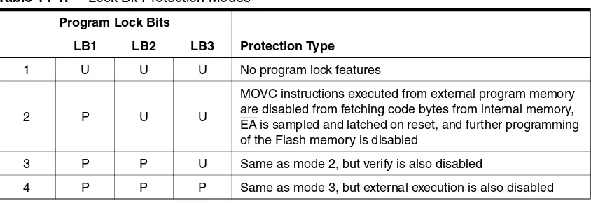
14. Program Memory Lock Bits
The AT89S51 has three lock bits that can be left unprogrammed (U) or can be programmed (P) to obtain the additional features listed in Table 14-1.
When lock bit 1 is programmed, the logic level at the EA pin is sampled and latched during reset. If the device is powered up without a reset, the latch initializes to a random value and holds that value until reset is activated. The latched value of EA must agree with the current logic level at that pin in order for the device to function properly.
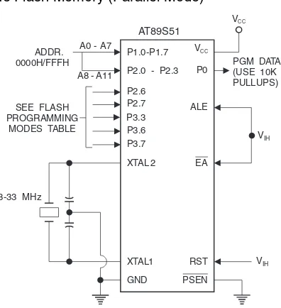
15. Programming the Flash – Parallel Mode
The AT89S51 is shipped with the on-chip Flash memory array ready to be programmed. The programming interface needs a high-voltage (12-volt) program enable signal and is compatible with conventional third-party Flash or EPROM programmers.
The AT89S51 code memory array is programmed byte-by-byte.
Programming Algorithm: Before programming the AT89S51, the address, data, and control signals should be set up according to the Flash Programming Modes table (Table 17-1) and
Fig-ure 17-1 and Figure 17-2. To program the AT89S51, take the following steps:
1. Input the desired memory location on the address lines. 2. Input the appropriate data byte on the data lines. 3. Activate the correct combination of control signals. 4. Raise EA/VPP to 12V.
5. Pulse ALE/PROG once to program a byte in the Flash array or the lock bits. The byte-write cycle is self-timed and typically takes no more than 50 µs. Repeat steps 1 through 5, changing the address and data for the entire array or until the end of the object file is reached.
Data Polling: The AT89S51 features Data Polling to indicate the end of a byte write cycle. Dur-ing a write cycle, an attempted read of the last byte written will result in the complement of the written data on P0.7. Once the write cycle has been completed, true data is valid on all outputs, and the next cycle may begin. Data Polling may begin any time after a write cycle has been initiated.
Table 14-1. Lock Bit Protection Modes Program Lock Bits
LB1 LB2 LB3 Protection Type
1 U U U No program lock features
2 P U U
MOVC instructions executed from external program memory are disabled from fetching code bytes from internal memory, EA is sampled and latched on reset, and further programming of the Flash memory is disabled
3 P P U Same as mode 2, but verify is also disabled
Program Verify: If lock bits LB1 and LB2 have not been programmed, the programmed code data can be read back via the address and data lines for verification. The status of the individ-ual lock bits can be verified directly by reading them back.
Reading the Signature Bytes: The signature bytes are read by the same procedure as a nor-mal verification of locations 000H, 100H, and 200H, except that P3.6 and P3.7 must be pulled to a logic low. The values returned are as follows.
(000H) = 1EH indicates manufactured by Atmel (100H) = 51H indicates AT89S51
(200H) = 06H
Chip Erase: In the parallel programming mode, a chip erase operation is initiated by using the proper combination of control signals and by pulsing ALE/PROG low for a duration of 200 ns - 500 ns.
In the serial programming mode, a chip erase operation is initiated by issuing the Chip Erase instruction. In this mode, chip erase is self-timed and takes about 500 ms.
During chip erase, a serial read from any address location will return 00H at the data output.
16. Programming the Flash – Serial Mode
The Code memory array can be programmed using the serial ISP interface while RST is pulled to VCC. The serial interface consists of pins SCK, MOSI (input) and MISO (output). After RST is
set high, the Programming Enable instruction needs to be executed first before other operations can be executed. Before a reprogramming sequence can occur, a Chip Erase operation is required.
The Chip Erase operation turns the content of every memory location in the Code array into FFH.
Either an external system clock can be supplied at pin XTAL1 or a crystal needs to be connected across pins XTAL1 and XTAL2. The maximum serial clock (SCK) frequency should be less than 1/16 of the crystal frequency. With a 33 MHz oscillator clock, the maximum SCK frequency is 2 MHz.
16.1
Serial Programming Algorithm
To program and verify the AT89S51 in the serial programming mode, the following sequence is recommended:
1. Power-up sequence:
a. Apply power between VCC and GND pins. b. Set RST pin to “H”.
If a crystal is not connected across pins XTAL1 and XTAL2, apply a 3 MHz to 33 MHz clock to XTAL1 pin and wait for at least 10 milliseconds.
2. Enable serial programming by sending the Programming Enable serial instruction to pin MOSI/P1.5. The frequency of the shift clock supplied at pin SCK/P1.7 needs to be less than the CPU clock at XTAL1 divided by 16.
3. The Code array is programmed one byte at a time in either the Byte or Page mode. The write cycle is self-timed and typically takes less than 0.5 ms at 5V.
5. At the end of a programming session, RST can be set low to commence normal device operation.
Power-off sequence (if needed):
1. Set XTAL1 to “L” (if a crystal is not used). 2. Set RST to “L”.
3. Turn VCC power off.
Data Polling: The Data Polling feature is also available in the serial mode. In this mode, during a write cycle an attempted read of the last byte written will result in the complement of the MSB of the serial output byte on MISO.
16.2
Serial Programming Instruction Set
The Instruction Set for Serial Programming follows a 4-byte protocol and is shown in the
”Serial Programming Instruction Set” on page 20.
17. Programming Interface – Parallel Mode
Every code byte in the Flash array can be programmed by using the appropriate combination of control signals. The write operation cycle is self-timed and once initiated, will automatically time itself to completion.
Most major worldwide programming vendors offer worldwide support for the Atmel AT89 micro-controller series. Please contact your local programming vendor for the appropriate software revision.
Table 17-1. Flash Programming Modes
Mode VCC RST PSEN
ALE/ PROG
EA/
VPP P2.6 P2.7 P3.3 P3.6 P3.7
P0.7-0 Data
P2.3-0 P1.7-0
Address
Write Code Data 5V H L
(2)
12V L H H H H DIN A11-8 A7-0
Read Code Data 5V H L H H L L L H H DOUT A11-8 A7-0
Write Lock Bit 1 5V H L
(3)
12V H H H H H X X X
Write Lock Bit 2 5V H L
(3)
12V H H H L L X X X
Write Lock Bit 3 5V H L
(3)
12V H L H H L X X X
Read Lock Bits
1, 2, 3 5V H L H H H H L H L
P0.2, P0.3, P0.4
X X
Chip Erase 5V H L
(1)
12V H L H L L X X X
Read Atmel ID 5V H L H H L L L L L 1EH 0000 00H
Read Device ID 5V H L H H L L L L L 51H 0001 00H
Figure 17-1. Programming the Flash Memory (Parallel Mode)
Figure 17-2. Verifying the Flash Memory (Parallel Mode)
P1.0-P1.7
P2.6
P3.6 P2.0 - P2.3 A0 - A7
ADDR. 0000H/FFFH
SEE FLASH PROGRAMMING
MODES TABLE
3-33 MHz
P0 V
P2.7
PGM DATA
PROG
V /VIH PP
VIH
ALE
P3.7
XTAL2 EA
RST PSEN XTAL1
GND
VCC
AT89S51
P3.3
P3.0 RDY/ BSY A8 - A11
CC
P1.0-P1.7
P2.6
P3.6 P2.0 - P2.3 A0 - A7
ADDR. 0000H/FFFH
SEE FLASH PROGRAMMING
MODES TABLE
3-33 MHz
P0
P2.7
PGM DATA (USE 10K PULLUPS)
VIH
VIH
ALE
P3.7
XTAL 2 EA
RST PSEN XTAL1
GND
VCC AT89S51
P3.3 A8 - A11
Figure 18-1. Flash Programming and Verification Waveforms – Parallel Mode
18. Flash Programming and Verification Characteristics (Parallel Mode)
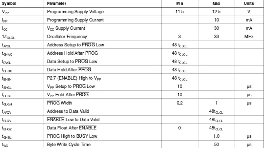
TA = 20°C to 30°C, VCC = 4.5 to 5.5VSymbol Parameter Min Max Units
VPP Programming Supply Voltage 11.5 12.5 V
IPP Programming Supply Current 10 mA
ICC VCC Supply Current 30 mA
1/tCLCL Oscillator Frequency 3 33 MHz
tAVGL Address Setup to PROG Low 48 tCLCL
tGHAX Address Hold After PROG 48 tCLCL
tDVGL Data Setup to PROG Low 48 tCLCL
tGHDX Data Hold After PROG 48 tCLCL
tEHSH P2.7 (ENABLE) High to VPP 48 tCLCL
tSHGL VPP Setup to PROG Low 10 µs
tGHSL VPP Hold After PROG 10 µs
tGLGH PROG Width 0.2 1 µs
tAVQV Address to Data Valid 48tCLCL
tELQV ENABLE Low to Data Valid 48tCLCL
tEHQZ Data Float After ENABLE 0 48tCLCL
tGHBL PROG High to BUSY Low 1.0 µs
tWC Byte Write Cycle Time 50 µs
tGLGH tGHSL
tAVGL
tSHGL
tDVGL
tGHAX
tAVQV
tGHDX
tEHSH t
ELQV
t
BUSY READY
tGHBL
tEHQZ P1.0 - P1.7
P2.0 - P2.3
ALE/PROG PORT 0
LOGIC 1 LOGIC 0
EA/VPP
VPP
P2.7 (ENABLE)
P3.0 (RDY/BSY)
PROGRAMMING ADDRESS
VERIFICATION ADDRESS
Figure 18-2. Flash Memory Serial Downloading
19. Flash Programming and Verification Waveforms – Serial Mode
Figure 19-1. Serial Programming Waveforms
P1.7/SCK DATA OUTPUT
INSTRUCTION INPUT
CLOCK IN
3-33 MHz
P1.5/MOSI
VIH
XTAL2
RST XTAL1
GND
VCC
AT89S51
P1.6/MISO
VCC
Note: 1. B1 = 0, B2 = 0
→
Mode 1, no lock protection B1 = 0, B2 = 1→
Mode 2, lock bit 1 activated B1 = 1, B2 = 0→
Mode 3, lock bit 2 activated B1 = 1, B2 = 1→
Mode 4, lock bit 3 activatedAfter Reset signal is high, SCK should be low for at least 64 system clocks before it goes high to clock in the enable data bytes. No pulsing of Reset signal is necessary. SCK should be no faster than 1/16 of the system clock at XTAL1.
For Page Read/Write, the data always starts from byte 0 to 255. After the command byte and upper address byte are latched, each byte thereafter is treated as data until all 256 bytes are shifted in/out. Then the next instruction will be ready to be decoded.
20. Serial Programming Instruction Set
Instruction
Instruction Format
Operation
Byte 1 Byte 2 Byte 3 Byte 4
Programming Enable 1010 1100 0101 0011 xxxx xxxx
xxxx xxxx 0110 1001 (Output on MISO)
Enable Serial Programming while RST is high
Chip Erase 1010 1100 100x xxxx xxxx xxxx xxxx xxxx Chip Erase Flash memory array
Read Program Memory
(Byte Mode) 0010 0000
xxxx Read data from Program
memory in the byte mode
Write Program Memory
(Byte Mode) 0100 0000
xxxx Write data to Program
memory in the byte mode
Write Lock Bits(1) 1010 1100 1110 00 xxxx xxxx xxxx xxxx Write Lock bits. See Note (1).
Read Lock Bits 0010 0100 xxxx xxxx xxxx xxxx xxx xx
Read back current status of the lock bits (a programmed lock bit reads back as a “1”)
Read Signature Bytes 0010 1000 xxxx xxx xxx0 Signature Byte Read Signature Byte
Read Program Memory
(Page Mode) 0011 0000
xxxx
Byte 0 Byte 1... Byte 255
Read data from Program memory in the Page Mode (256 bytes)
Write Program Memory
(Page Mode) 0101 0000 xxxx Byte 0
Byte 1... Byte 255
Write data to Program memory in the Page Mode (256 bytes)
}
Each of the lock bit modes need to be activated sequentially be-fore Mode 4 can be executed.D7 D6 D5 D4 D3 D2 D1 D0 A7 A6 A5 A4 A3 A2 A1 A0
A11 A10 A9 A8
B2
B1
A11 A10 A9 A8 A7 A6 A5 A4 A3 A2 A1 A0 D7 D6 D5 D4 D3 D2 D1 D0
LB3 LB2 LB
1
A1
1
A1
0
A9 A8
A1
1
A1
0
A9 A8
A7
A11 A1
0
21. Serial Programming Characteristics
Figure 21-1. Serial Programming Timing
MOSI
MISO
SCK
t
OVSHt
SHSLt
SLSHt
SHOXt
SLIVTable 21-1. Serial Programming Characteristics, TA = -40°C to 85°C, VCC = 4.0 - 5.5V (Unless Otherwise Noted)
Symbol Parameter Min Typ Max Units
1/tCLCL Oscillator Frequency 3 33 MHz
tCLCL Oscillator Period 30 ns
tSHSL SCK Pulse Width High 8 tCLCL ns
tSLSH SCK Pulse Width Low 8 tCLCL ns
tOVSH MOSI Setup to SCK High tCLCL ns
tSHOX MOSI Hold after SCK High 2 tCLCL ns
tSLIV SCK Low to MISO Valid 10 16 32 ns
tERASE Chip Erase Instruction Cycle Time 500 ms
tSWC Serial Byte Write Cycle Time 64 tCLCL + 400 µs
22. Absolute Maximum Ratings*
Operating Temperature... -55°C to +125°C *NOTICE: Stresses beyond those listed under “Absolute Maximum Ratings” may cause permanent dam-age to the device. This is a stress rating only and functional operation of the device at these or any other conditions beyond those indicated in the operational sections of this specification is not implied. Exposure to absolute maximum rating conditions for extended periods may affect device reliability.
Storage Temperature ... -65°C to +150°C
Voltage on Any Pin
with Respect to Ground ...-1.0V to +7.0V
Maximum Operating Voltage ... 6.6V
Notes: 1. Under steady state (non-transient) conditions, IOL must be externally limited as follows: Maximum IOL per port pin: 10 mA
Maximum IOL per 8-bit port:
Port 0: 26 mA Ports 1, 2, 3: 15 mA Maximum total IOL for all output pins: 71 mA
If IOL exceeds the test condition, VOL may exceed the related specification. Pins are not guaranteed to sink current greater than the listed test conditions.
2. Minimum VCC for Power-down is 2V.
23. DC Characteristics
The values shown in this table are valid for TA = -40°C to 85°C and VCC = 4.0V to 5.5V, unless otherwise noted.
Symbol Parameter Condition Min Max Units
VIL Input Low Voltage (Except EA) -0.5 0.2 VCC-0.1 V
VIL1 Input Low Voltage (EA) -0.5 0.2 VCC-0.3 V
VIH Input High Voltage (Except XTAL1, RST) 0.2 VCC+0.9 VCC+0.5 V
VIH1 Input High Voltage (XTAL1, RST) 0.7 VCC VCC+0.5 V
VOL Output Low Voltage(1) (Ports 1,2,3) IOL = 1.6 mA 0.45 V
VOL1 Output Low Voltage
(1)
(Port 0, ALE, PSEN) IOL = 3.2 mA 0.45 V
VOH
Output High Voltage (Ports 1,2,3, ALE, PSEN)
IOH = -60 µA, VCC = 5V ± 10% 2.4 V
IOH = -25 µA 0.75 VCC V
IOH = -10 µA 0.9 VCC V
VOH1 Output High Voltage
(Port 0 in External Bus Mode)
IOH = -800 µA, VCC = 5V ± 10% 2.4 V
IOH = -300 µA 0.75 VCC V
IOH = -80 µA 0.9 VCC V
IIL Logical 0 Input Current (Ports 1,2,3) VIN = 0.45V -50 µA
ITL Logical 1 to 0 Transition Current
(Ports 1,2,3) VIN = 2V, VCC = 5V ± 10% -300 µA
ILI Input Leakage Current (Port 0, EA) 0.45 < VIN < VCC ±10 µA
RRST Reset Pulldown Resistor 50 300 KΩ
CIO Pin Capacitance Test Freq. = 1 MHz, TA = 25°C 10 pF
ICC
Power Supply Current Active Mode, 12 MHz 25 mA
Idle Mode, 12 MHz 6.5 mA
Power-down Mode(2) V
24. AC Characteristics
Under operating conditions, load capacitance for Port 0, ALE/PROG, and PSEN = 100 pF; load capacitance for all other outputs = 80 pF.
24.1
External Program and Data Memory Characteristics
Symbol Parameter
12 MHz Oscillator Variable Oscillator
Units
Min Max Min Max
1/tCLCL Oscillator Frequency 0 33 MHz
tLHLL ALE Pulse Width 127 2 tCLCL-40 ns
tAVLL Address Valid to ALE Low 43 tCLCL-25 ns
tLLAX Address Hold After ALE Low 48 tCLCL-25 ns
tLLIV ALE Low to Valid Instruction In 233 4 tCLCL-65 ns
tLLPL ALE Low to PSEN Low 43 tCLCL-25 ns
tPLPH PSEN Pulse Width 205 3 tCLCL-45 ns
tPLIV PSEN Low to Valid Instruction In 145 3 tCLCL-60 ns
tPXIX Input Instruction Hold After PSEN 0 0 ns
tPXIZ Input Instruction Float After PSEN 59 tCLCL-25 ns
tPXAV PSEN to Address Valid 75 tCLCL-8 ns
tAVIV Address to Valid Instruction In 312 5 tCLCL-80 ns
tPLAZ PSEN Low to Address Float 10 10 ns
tRLRH RD Pulse Width 400 6 tCLCL-100 ns
tWLWH WR Pulse Width 400 6 tCLCL-100 ns
tRLDV RD Low to Valid Data In 252 5 tCLCL-90 ns
tRHDX Data Hold After RD 0 0 ns
tRHDZ Data Float After RD 97 2 tCLCL-28 ns
tLLDV ALE Low to Valid Data In 517 8 tCLCL-150 ns
tAVDV Address to Valid Data In 585 9 tCLCL-165 ns
tLLWL ALE Low to RD or WR Low 200 300 3 tCLCL-50 3 tCLCL+50 ns
tAVWL Address to RD or WR Low 203 4 tCLCL-75 ns
tQVWX Data Valid to WR Transition 23 tCLCL-30 ns
tQVWH Data Valid to WR High 433 7 tCLCL-130 ns
tWHQX Data Hold After WR 33 tCLCL-25 ns
tRLAZ RD Low to Address Float 0 0 ns
25. External Program Memory Read Cycle
26. External Data Memory Read Cycle
tLHLL
tLLIV
tPLIV
tLLAX tPXIZ
tPLPH
tPLAZ
tPXAV tAVLL
tLLPL
tAVIV
tPXIX ALE
PSEN
PORT 0
PORT 2 A8 - A15
A0 - A7 A0 - A7
A8 - A15 INSTR IN
tLHLL
tLLDV
tLLWL
tLLAX
tWHLH
tAVLL
tRLRH
tAVDV
tAVWL
tRLAZ t
RHDX
tRLDV tRHDZ
A0 - A7 FROM RI OR DPL
ALE
PSEN
RD
PORT 0
PORT 2 P2.0 - P2.7 OR A8 - A15 FROM DPH
A0 - A7 FROM PCL
A8 - A15 FROM PCH
27. External Data Memory Write Cycle
28. External Clock Drive Waveforms
tLHLL
tLLWL
tLLAX
tWHLH
tAVLL
tWLWH
tAVWL tQVWX
tQVWH
tWHQX
A0 - A7 FROM RI OR DPL
ALE
PSEN
WR
PORT 0
PORT 2 P2.0 - P2.7 OR A8 - A15 FROM DPH
A0 - A7 FROM PCL
A8 - A15 FROM PCH
DATA OUT INSTR IN
tCHCX
tCHCX
tCLCX
tCLCL
tCHCL
tCLCH
V - 0.5VCC
0.45V
0.2 VCC- 0.1V 0.7 VCC
29. External Clock Drive
Symbol Parameter Min Max Units
1/tCLCL Oscillator Frequency 0 33 MHz
tCLCL Clock Period 30 ns
tCHCX High Time 12 ns
tCLCX Low Time 12 ns
tCLCH Rise Time 5 ns
31. Shift Register Mode Timing Waveforms
32. AC Testing Input/Output Waveforms
(1)Note: 1. AC Inputs during testing are driven at VCC - 0.5V for a logic 1 and 0.45V for a logic 0. Timing measurements are made at VIH min. for a logic 1 and VIL max. for a logic 0.
33. Float Waveforms
(1)Note: 1. For timing purposes, a port pin is no longer floating when a 100 mV change from load voltage occurs. A port pin begins to float when a 100 mV change from the loaded VOH/VOL level occurs.
30. Serial Port Timing: Shift Register Mode Test Conditions
The values in this table are valid for VCC = 4.0V to 5.5V and Load Capacitance = 80 pF.Symbol Parameter
12 MHz Osc Variable Oscillator
Units
Min Max Min Max
tXLXL Serial Port Clock Cycle Time 1.0 12 tCLCL µs
tQVXH Output Data Setup to Clock Rising Edge 700 10 tCLCL-133 ns
tXHQX Output Data Hold After Clock Rising Edge 50 2 tCLCL-80 ns
tXHDX Input Data Hold After Clock Rising Edge 0 0 ns
tXHDV Clock Rising Edge to Input Data Valid 700 10 tCLCL-133 ns
tXHDV
tQVXH
tXLXL
tXHDX
tXHQX
ALE
INPUT DATA CLEAR RI OUTPUT DATA
WRITE TO SBUF
INSTRUCTION
CLOCK
0
0 1
1 2
2 3
3 4
4 5
5 6
6 7
7
SET TI
SET RI 8
VALID VALID VALID VALID VALID VALID VALID VALID
0.45V
TEST POINTS V - 0.5VCC
0.2 V + 0.9VCC
0.2 V - 0.1VCC
VLOAD+ 0.1V
Timing Reference Points V
LOAD- 0.1V LOAD
V VOL+ 0.1V
34. Ordering Information
34.1
Standard Package
Speed (MHz)
Power
Supply Ordering Code Package Operation Range
24 4.0V to 5.5V
AT89S51-24AC AT89S51-24JC AT89S51-24PC AT89S51-24SC
44A 44J 40P6 42PS6
Commercial (0°C to 70°C)
AT89S51-24AI AT89S51-24JI AT89S51-24PI AT89S51-24SI
44A 44J 40P6 42PS6
Industrial (-40°C to 85°C)
33 4.5V to 5.5V
AT89S51-33AC AT89S51-33JC AT89S51-33PC AT89S51-33SC
44A 44J 40P6 42PS6
Commercial (0°C to 70°C)
34.2
Green Package Option (Pb/Halide-free)
Speed (MHz)
Power
Supply Ordering Code Package Operation Range
24 4.0V to 5.5V
AT89S51-24AU AT89S51-24JU AT89S51-24PU
44A 44J 40P6
Industrial (-40°C to 85°C)
Package Type 44A 44-lead, Thin Plastic Gull Wing Quad Flatpack (TQFP) 44J 44-lead, Plastic J-leaded Chip Carrier (PLCC)
35. Packaging Information
35.1
44A – TQFP
10/5/2001
PIN 1 IDENTIFIER
0˚~7˚ PIN 1
L C
A1 A2 A
D1 D
e E1 E
B
COMMON DIMENSIONS
(Unit of Measure = mm)
SYMBOL MIN NOM MAX NOTE
Notes: 1. This package conforms to JEDEC reference MS-026, Variation ACB. 2. Dimensions D1 and E1 do not include mold protrusion. Allowable
protrusion is 0.25 mm per side. Dimensions D1 and E1 are maximum plastic body size dimensions including mold mismatch.
3. Lead coplanarity is 0.10 mm maximum.
A – – 1.20
A1 0.05 – 0.15
A2 0.95 1.00 1.05
D 11.75 12.00 12.25
D1 9.90 10.00 10.10 Note 2
E 11.75 12.00 12.25
E1 9.90 10.00 10.10 Note 2
B 0.30 – 0.45
C 0.09 – 0.20
L 0.45 – 0.75
35.2
44J – PLCC
Notes: 1. This package conforms to JEDEC reference MS-018, Variation AC.
2. Dimensions D1 and E1 do not include mold protrusion. Allowable protrusion is .010"(0.254 mm) per side. Dimension D1 and E1 include mold mismatch and are measured at the extreme material condition at the upper or lower parting line.
3. Lead coplanarity is 0.004" (0.102 mm) maximum.
A 4.191 – 4.572
A1 2.286 – 3.048
A2 0.508 – –
D 17.399 – 17.653
D1 16.510 – 16.662 Note 2
E 17.399 – 17.653
E1 16.510 – 16.662 Note 2
D2/E2 14.986 – 16.002
B 0.660 – 0.813
B1 0.330 – 0.533
e 1.270 TYP
COMMON DIMENSIONS
(Unit of Measure = mm)
SYMBOL MIN NOM MAX NOTE
1.14(0.045) X 45˚ PIN NO. 1 IDENTIFIER
1.14(0.045) X 45˚
0.51(0.020)MAX
0.318(0.0125) 0.191(0.0075)
A2
45˚ MAX (3X)
A
A1
B1 D2/E2
B
e
E1 E
D1 D
44J, 44-lead, Plastic J-leaded Chip Carrier (PLCC) 44J B
10/04/01
2325 Orchard Parkway San Jose, CA 95131
TITLE DRAWING NO.
R
35.3
40P6 – PDIP
2325 Orchard Parkway
TITLE DRAWING NO. REV.
40P6, 40-lead (0.600"/15.24 mm Wide) Plastic Dual 40P6 B 09/28/01 PIN
1
E1
A1
B
REF E
B1
C L
SEATING PLANE
A
0º ~ 15º D
e
eB
COMMON DIMENSIONS
(Unit of Measure = mm)
SYMBOL MIN NOM MAX NOTE
A – – 4.826
A1 0.381 – –
D 52.070 – 52.578 Note 2
E 15.240 – 15.875
E1 13.462 – 13.970 Note 2
B 0.356 – 0.559
B1 1.041 – 1.651
L 3.048 – 3.556
C 0.203 – 0.381
eB 15.494 – 17.526
e 2.540 TYP
Notes: 1. This package conforms to JEDEC reference MS-011, Variation AC. 2. Dimensions D and E1 do not include mold Flash or Protrusion.
35.4
42PS6 – PDIP
2325 Orchard Parkway San Jose, CA 95131
TITLE DRAWING NO.
R
REV. 42PS6, 42-lead (0.600"/15.24 mm Wide) Plastic Dual
Inline Package (PDIP) 42PS6 A
11/6/03 PIN
1
E1
A1
B
REF E
B1
C L
SEATING PLANE
A
0º ~ 15º D
e
eB
COMMON DIMENSIONS
(Unit of Measure = mm)
SYMBOL MIN NOM MAX NOTE
A – – 4.83
A1 0.51 – –
D 36.70 – 36.96 Note 2
E 15.24 – 15.88
E1 13.46 – 13.97 Note 2
B 0.38 – 0.56
B1 0.76 – 1.27
L 3.05 – 3.43
C 0.20 – 0.30
eB – – 18.55
e 1.78 TYP
Notes: 1. This package conforms to JEDEC reference MS-011, Variation AC. 2. Dimensions D and E1 do not include mold Flash or Protrusion.
Disclaimer: The information in this document is provided in connection with Atmel products. No license, express or implied, by estoppel or otherwise, to any intellectual property right is granted by this document or in connection with the sale of Atmel products. EXCEPT AS SET FORTH IN ATMEL’S TERMS AND CONDI-TIONS OF SALE LOCATED ON ATMEL’S WEB SITE, ATMEL ASSUMES NO LIABILITY WHATSOEVER AND DISCLAIMS ANY EXPRESS, IMPLIED OR STATUTORY WARRANTY RELATING TO ITS PRODUCTS INCLUDING, BUT NOT LIMITED TO, THE IMPLIED WARRANTY OF MERCHANTABILITY, FITNESS FOR A PARTICULAR PURPOSE, OR NON-INFRINGEMENT. IN NO EVENT SHALL ATMEL BE LIABLE FOR ANY DIRECT, INDIRECT, CONSEQUENTIAL, PUNITIVE, SPECIAL OR INCIDEN-TAL DAMAGES (INCLUDING, WITHOUT LIMITATION, DAMAGES FOR LOSS OF PROFITS, BUSINESS INTERRUPTION, OR LOSS OF INFORMATION) ARISING OUT OF THE USE OR INABILITY TO USE THIS DOCUMENT, EVEN IF ATMEL HAS BEEN ADVISED OF THE POSSIBILITY OF SUCH DAMAGES. Atmel makes no representations or warranties with respect to the accuracy or completeness of the contents of this document and reserves the right to make changes to specifications and product descriptions at any time without notice. Atmel does not make any commitment to update the information contained herein. Atmel’s products are not intended, authorized, or warranted for use as components in applications intended to support or sustain life.
Atmel Corporation
Atmel Operations
2325 Orchard Parkway San Jose, CA 95131, USA Tel: 1(408) 441-0311 Fax: 1(408) 487-2600
Regional Headquarters
Europe
Atmel Sarl
Route des Arsenaux 41 Case Postale 80 CH-1705 Fribourg Switzerland
Tel: (41) 26-426-5555 Fax: (41) 26-426-5500
Asia
Room 1219
Chinachem Golden Plaza 77 Mody Road Tsimshatsui East Kowloon
Hong Kong
Tel: (852) 2721-9778 Fax: (852) 2722-1369
Japan
9F, Tonetsu Shinkawa Bldg. 1-24-8 Shinkawa
Chuo-ku, Tokyo 104-0033 Japan
Tel: (81) 3-3523-3551 Fax: (81) 3-3523-7581
Memory
2325 Orchard Parkway San Jose, CA 95131, USA Tel: 1(408) 441-0311 Fax: 1(408) 436-4314
Microcontrollers
2325 Orchard Parkway San Jose, CA 95131, USA Tel: 1(408) 441-0311 Fax: 1(408) 436-4314
La Chantrerie BP 70602
44306 Nantes Cedex 3, France Tel: (33) 2-40-18-18-18
Fax: (33) 2-40-18-19-60
ASIC/ASSP/Smart Cards
Zone Industrielle
13106 Rousset Cedex, France Tel: (33) 4-42-53-60-00 Fax: (33) 4-42-53-60-01
1150 East Cheyenne Mtn. Blvd. Colorado Springs, CO 80906, USA Tel: 1(719) 576-3300
Fax: 1(719) 540-1759
Scottish Enterprise Technology Park Maxwell Building
East Kilbride G75 0QR, Scotland Tel: (44) 1355-803-000
Fax: (44) 1355-242-743
RF/Automotive
Theresienstrasse 2 Postfach 3535
74025 Heilbronn, Germany Tel: (49) 71-31-67-0 Fax: (49) 71-31-67-2340
1150 East Cheyenne Mtn. Blvd. Colorado Springs, CO 80906, USA Tel: 1(719) 576-3300
Fax: 1(719) 540-1759
Biometrics/Imaging/Hi-Rel MPU/ High Speed Converters/RF Datacom
Avenue de Rochepleine BP 123
38521 Saint-Egreve Cedex, France Tel: (33) 4-76-58-30-00
Fax: (33) 4-76-58-34-80