ANALOG CIRCUITS AND SIGNAL PROCESSING Consulting Editor: Mohammed Ismail. Ohio State University
Related Titles:
OPERATIONAL AMPLIFIER SPEED AND ACCURACY IMPROVEMENT
Ivanov and Filanovsky ISBN: 1-4020-7772-6
STATIC AND DYNAMIC PERFORMANCE LIMITATIONS FOR HIGH SPEED D/A CONVERTERS
van den Bosch, Steyaert and Sansen ISBN: 1-4020-7761-0
DESIGN AND ANALYSIS OF HIGH EFFICIENCY LINE DRIVERS FOR Xdsl
Piessens and Steyaert ISBN: 1-4020-7727-0
LOW POWER ANALOG CMOS FOR CARDIAC PACEMAKERS
Silveira and Flandre ISBN: 1-4020-7719-X
MIXED-SIGNAL LAYOUT GENERATION CONCEPTS
Lin, van Roermund, Leenaerts ISBN: 1-4020-7598-7
HIGH-FREQUENCY OSCILLATOR DESIGN FOR INTEGRATED TRANSCEIVERS
Van der Tang, Kasperkovitz and van Roermund ISBN: 1-4020-7564-2
CMOS INTEGRATION OF ANALOG CIRCUITS FOR HIGH DATA RATE TRANSMITTERS
DeRanter and Steyaert ISBN: 1-4020-7545-6
SYSTEMATIC DESIGN OF ANALOG IP BLOCKS
Vandenbussche and Gielen ISBN: 1-4020-7471-9
SYSTEMATIC DESIGN OF ANALOG IP BLOCKS
Cheung & Luong ISBN: 1-4020-7466-2
LOW-VOLTAGE CMOS LOG COMPANDING ANALOG DESIGN
Serra-Graells, Rueda & Huertas ISBN: 1-4020-7445-X
CIRCUIT DESIGN FOR WIRELESS COMMUNICATIONS
Pun, Franca & Leme ISBN: 1-4020-7415-8
DESIGN OF LOW-PHASE CMOS FRACTIONAL-N SYNTHESIZERS
DeMuer & Steyaert ISBN: 1-4020-7387-9
MODULAR LOW-POWER, HIGH SPEED CMOS ANALOG-TO-DIGITAL CONVERTER FOR EMBEDDED SYSTEMS
Lin, Kemna & Hosticka ISBN: 1-4020-7380-1
DESIGN CRITERIA FOR LOW DISTORTION IN FEEDBACK OPAMP CIRCUITE
Hernes & Saether ISBN: 1-4020-7356-9
CIRCUIT TECHNIQUES FOR LOW-VOLTAGE AND HIGH-SPEED A/D CONVERTERS
Walteri
ISBN: 1-4020-7244-9
DESIGN OF HIGH-PERFORMANCE CMOS VOLTAGE CONTROLLED OSCILLATORS
Dai and Harjani ISBN: 1-4020-7238-4
CMOS CIRCUIT DESIGN FOR RF SENSORS
Edgar Sánchez-Sinencio
CMOS PLL
Synthesizers:
Analysis and
Design
Print ©2005 Springer Science + Business Media, Inc.
All rights reserved
No part of this eBook may be reproduced or transmitted in any form or by any means, electronic, mechanical, recording, or otherwise, without written consent from the Publisher
Created in the United States of America Boston
©2005 Springer Science + Business Media, Inc.
Visit Springer's eBookstore at: http://ebooks.kluweronline.com
List of Acronyms and Symbols ix
2 Frequency Synthesizer for Wireless Applications
2.1 DEFINITION AND CHARACTERISTICS
2.2 PHASE NOISE AND TIMING JITTER
7 7 8
2.2.1 Phase noise and spurious tone 8
2.2.2 Timing jitter
2.3 IMPLEMENTATION OF FREQUENCY SYNTHESIZER
11 14
2.3.1 Direct analog frequency synthesizer 14
15 2.3.2 Direct digital frequency synthesizer
2.3.3 PLL-based frequency synthesizer 2.3.4 DLL-based frequency synthesizer 2.3.5 Hybrid frequency synthesizer
2.3.6 Summary and comparison of synthesizers
2.4 FREQUENCY SYNTHESIZER FOR WIRELESS TRANSCEIVERS
2.5 OTHER APPLICATIONS OF PLL AND FREQUENCY SYNTHESIZER
3 PLL Frequency Synthesizer 31 3.1 PLL FREQUENCY SYNTHESIZER BASICS
3.1.1 Basic building blocks of charge-pump PLL 3.1.2 Continuous-time linear phase analysis 3.1.3 Locking time
3.1.4 Tracking and acquisition 3.2 FAST-LOCKING TECHNIQUES
3.2.1 Bandwidth gear-shifting 3.2.2 VCO pre-tuning
3.3 DISCRETE-TIME ANALYSIS AND NONLINEAR MODELING
3.3.1 3.3.2
z-domain transfer function and stability analysis Nonlinear dynamic behavior modeling
3.4 DESIGN EXAMPLE: 2.4GHZ INTEGER-N PLL FOR BLUETOOTH
REFERENCES
4 Fractional-N PLL Synthesizer 69 69 4.1 FRACTIONAL-N FREQUENCY SYNTHESIZER
4.1.1 quantization noise to phase noise mapping 4.1.2 quantization noise to timing jitter mapping 4.2 ACOMPARATIVE STUDY OF DIGITAL MODULATORS
4.2.1 Design considerations
4.2.2 Four types of digital modulators 4.2.3 Summary of comparative study 4.3 OTHER APPLICATIONS OF
4.3.1 Direct digital modulation 4.3.2 Frequency-to-digital conversion 4.4 MODELING AND SIMULATION OF
4.5 DESIGN EXAMPLE:900MHz FOR GSM REFERENCES
5 Enhanced Phase Switching Prescaler 103 103
Summary and comparison of prescalers 5.2
5.3
ENHANCED PHASE-SWITCHING PRESCALER
CIRCUIT DESIGN AND SIMULATION RESULTS
5.3.1 5.3.2 5.3.3 5.3.4
Eight 45°-spaced phases generation 8-to-1 multiplexer
Switching control circuit
Asynchronous frequency divider
5.5 SPURS DUE TO NONIDEAL45° PHASE SPACING
REFERENCES
117 123
6 Loop Filter With Capacitance Multiplier 127 127 6.1 LOOP FILTER ARCHITECTURE
6.1.1
Summary and comparison of loop filters 6.2
6.3
LOOP FILTER AND CHARGE-PUMP NOISE MAPPING
LOOP FILTER WITH CAPACITANCE MULTIPLIER
6.3.1
Simulation of loop filter with capacitance multiplier Noise consideration
REFERENCES
7 Other Building Blocks of PLL 151 151
AAC
MASH
angular frequency in rad/s
PLL –3dB loop bandwidth
PLL loop (unity-gain / crossover) bandwidth
corner frequency of capacitance multiplier impedance corner frequency of capacitance multiplier impedance corner frequency of capacitance multiplier impedance natural frequency
pole-frequency of loop filter transimpedance
pole-frequency of loop filter transimpedance
pole-frequency of loop filter transimpedance
PLL reference angular frequency (at PFD)
zero-frequency of loop filter
corner angular frequency of 1/f noise
angular frequency offset from carrier PLL output rms phase noise phase
phase error at PFD inputs
input phase (noise) output phase (noise) VCO phase noise random phase variation damping factor
normalized settling frequency error of PLL phase noise in dBc/Hz
rms of cycle jitter
rms of cycle-to-cycle jitter time
impulse function (Dirac delta function) periodic impulse function with period T
ISF function
B
f
current ratio
capacitance of passive loop filter capacitance of passive loop filter capacitance of passive loop filter
parasitic capacitance of capacitance multiplier
parasitic capacitance of capacitance multiplier
frequency in Hz
carrier frequency
PLL loop (unity-gain / crossover) bandwidth loop divider output frequency
PLL reference frequency (at PFD)
VCO frequency
RF frequency (of mixer) local oscillator frequency offset frequency from the carrier
corner frequency of oscillator phase noise
F g G h H
active device noise factor conductance, transconductance conductance, transconductance transfer function
transfer function
PLL closed-loop input-to-output phase (noise) transfer function
PLL input phase (noise) to PFD phase error transfer function
PLL open-loop input-to-output phase (noise) transfer function
PLL input phase to LF output voltage transfer function
i current
control current of CCO charge-pump current
charge-pump current of integration path
charge-pump current of proportional path
charge-pump current for discharging the load capacitor output current of LF’s proportional path
charge-pump current for charging the load capacitor
output current of LF’s integration path integer number
binary integer input of DPA or digital SDM Boltzmann constant
PLL loop gain
PFD and charge-pump gain in A/rad
VCO conversion gain in rad/s/V
L
integer number (order of SDM) inductance
integer number
modulus of DPA or digital SDM integer number
output integer of digital SDM
number
(nominal) frequency divide ratio of loop divider integer part of fractional-N divide ratio
prescaler divide ratio power
PLL reference spur level in dBc
charge
resistance of passive loop filter
resistance of passive loop filter
auto-correlation function of random phase
power spectrum
power spectral density of random phase variation
power spectral density of signal V(t) time
charge-pump turn-on time in locked state time
temperature
PLL lock-in time (rough estimation) PLL pull-in time
period of PLL reference signal
y z Z
VCO control voltage, LF output voltage output voltage of LF’s proportional path
output voltage of LF’s integration path loop filter output voltage noise
admittance impedance
Thanks to the advance of semiconductor and communication technology, the wireless communication market has been booming in the last two decades. It evolved from simple pagers to emerging third-generation (3G) cellular phones. In the meanwhile, broadband communication market has also gained a rapid growth. As the market always demands performance and low-cost products, circuit designers are seeking high-integration communication devices in cheap CMOS technology.
The phase-locked loop frequency synthesizer is a critical component in communication devices. It works as a local oscillator for frequency translation and channel selection in wireless transceivers and broadband cable tuners. It also plays an important role as the clock synthesizer for data converters in the analog-and-digital signal interface.
This book covers the design and analysis of PLL synthesizers. It includes both fundamentals and a review of the state-of-the-art techniques. The transient analysis of the third-order charge-pump PLL reveals its locking behavior accurately. The behavioral-level simulation of PLL further clarifies its stability limit. Design examples are given to clearly illustrate the design procedure of PLL synthesizers. A complete derivation of reference spurs in the charge-pump PLL is also presented in this book.
prescaler might be a concern, it is mathematically examined. Another single chapter in this book is devoted to the loop filter, which is an integration bottleneck in narrow-band PLL because its big capacitor takes a large chip area. A simple area-efficient on-chip loop filter solution was proposed. It is based on a capacitance multiplier, which is of very low complexity and power consumption. Detailed analysis and design of this novel loop filter was addressed.
INTRODUCTION
1.1
Motivation
In the last decade, the rapid growth of wireless applications has led to an increasing demand of fully integrated, low-cost, low-power, and high-performance transceivers. The applications of wireless communication devices include pagers, cordless phones, cellular phones, global positioning systems (GPS), and wireless local area networks (WLAN), transmitting either voice or data. A standard specifies how devices talk to each other. Numerous standards emerged and are optimized for certain applications. For voice, examples include AMPS, NMT, TACS, D-AMPS, DECT, GSM, DCS, PCS, PDC, TDMA, CDMA, etc. It has evolved from analog to digital, from the 1G (first generation) to the current existing 2.5G, such as GPRS and EDGE. Devices in the 3G wireless standards, which include UMTS (WCDMA), CDMA2000 and TD-SCDMA, are also emerging in some areas of the world. For data, there are 802.11a/b/g WLAN, HiperLAN, Bluetooth, HomeRF, and so on. More recently, a significant interest has grown in the ultra wideband communications [1], [2]. Figure 1-1 briefly illustrates the frequency band of some wireless communication standards.
design the radio frequency integrated circuits (RFIC) in CMOS technology. A single-chip transceiver with a minimum number of off-chip components is preferred to reduce the cost and size of wireless devices, like cellular phones [3]-[7].
Figure 1-1. Frequency band of wireless communication standards
There are still many difficulties, however, in the process of integration of RF front-end due to the lack of high-quality components on chip. This book focuses on the design of the frequency synthesizer, one of the key building blocks of the RF front-end in CMOS technology. The frequency synthesizer is used as a local oscillator for frequency translation and channel selection in the RF front-end of wireless transceivers. It is a critical component in terms of the performance and cost of a wireless transceiver [8].
1.2
Summary of book
This book focuses on both fundamentals and advanced design techniques of PLL-based frequency synthesizers. A 2.4GHz fully integrated fractional-N frequency synthesizer prototype is implemented in
CMOS technology. Efforts have been put on the prescaler and loop filter, which are the speed and integration bottlenecks, respectively.
A low-power and robust prescaler using an enhanced phase-switching architecture was proposed [9]-[12]. The new architecture is based on generating eight 45°-spaced phases and judiciously arranging the phase-switching sequence to yield an inherently glitch-free phase-phase-switching operation.
reduced by half, from 1/4 to 1/8 of the prescaler’s input frequency, the MUX can be implemented with standard digital cells to save power consumption and the robustness of phase-switching operation is improved.
Furthermore, the main problem associated with the existing phase-switching architecture is the potential glitches if the phase-switching occurs in the incorrect timing window. Thus, various significant efforts have been made in the literature to yield a glitch-free phase-switching prescaler [13]-[16]. However, all these glitch-removing schemes are not robust and often cost considerable power and area, or even sacrifice the prescaler’s maximum operating speed. But in the proposed enhanced phase-switching architecture, an inherently glitch-free phase-switching operation is obtained by means of reversing the switching sequence. Thus, no retiming or synchronization circuit is needed for the switching control and the robustness of the switching operation is guaranteed.
To provide a further insight into the switching operation in the proposed phase-switching architecture, a detailed delay timing analysis of the switching control loop is given. By calculating the delay budget in the loop, we conclude that usually the first ÷2 divider is the only speed constraint of this enhanced phase-switching architecture.
The loop filter is a barrier in fully integrating a narrow-band PLL because of its large integrating capacitor. To make the loop capacitance of a narrow-band PLL as small as possible while keeping the same loop narrow-bandwidth, designers increase the loop resistance and reduce the charge-pump current. However, there are practical limitations for both the loop resistance and the charge-pump current. Thermal noise in the large resistor modulates the control voltage and generates phase noise in the VCO, and the charge-pump noise increases while the current decreases.
The dual-path topology has been a popular solution to this problem [17]-[22]. It equivalently scales down the largest integrating and zero-generating capacitance by the scaling factor of the dual charge-pump currents. Besides the increased noise and power due to active devices, the charge-pump of the integration path is still working with a very small current and contributes significant noise. Also, the delay mismatch of the dual charge-pumps may change the loop parameters. Furthermore, at least for the implementations in [18]-[20] and [22], the voltage decay of the low-pass path causes undesirable ripples on the VCO control voltage.
To overcome the constraints of the dual-path topology, a novel loop filter solution is proposed [10]-[12]. A capacitance multiplier [23] is used to reduce the capacitance by a large factor and make it easily integratable within a small chip area.
three-level digital modulator is employed to reduce the instantaneous phase error at the PFD. The folding of the phase noise is minimized by reducing nonlinearities of the PFD and charge pump [10]-[12],
[24].
Furthermore, the derivation of the settling time of the third-order PLL, the derivation of spurs due to delay/phase mismatches in the phase-switching prescaler, a complete analysis of the reference spur in the charge-pump PLL, and the behavioral-level verification of the PLL stability limit are all presented in this book.
A prototype chip of the PLL synthesizer was fabricated in TSMC 4-metal 2-poly (4M2P) CMOS process through MOSIS. The die size is 2mm×2mm. It includes a fully integrated fractional-N frequency synthesizer and some standalone building blocks for testing. The PLL takes an active area of of which the digital modulator occupies With a power supply of 1.5-V for VCO and prescaler, and 2.0-V for other blocks, the whole PLL system consumes 16mW, of which the VCO consumes 9mW. With the reference frequency of 50MHz, the measured phase noise is –128dBc/Hz at 10MHz offset and the reference spur is – 57dBc.
The proposed prescaler only takes an area of With a 1.5- V
power supply, it works well within the PLL’s tuning range of 2.23~2.45GHz
and consumes 3mW. The proposed loop filter occupies and its power consumption (0.2mW) and noise are negligible compared with the
whole PLL.
1.3
Book organization
In Chapter 2, the fundamentals of the frequency synthesizer including its features, applications, implementations, and key parameters (jitter and phase noise) are reviewed. Various synthesizer architectures and their pros and cons are discussed.
In Chapter 3, the analysis of the PLL-based frequency synthesizer is covered. It includes the continuous-time linear analysis, discrete-time analysis, stability concerns, operation modes, and fast-locking techniques, etc. An integer-N PLL frequency synthesizer design example is given to illustrate the design procedure.
Chapter 5 is devoted to the design of the prescaler. The existing design techniques are overviewed. An enhanced, inherently glitch-free phase-switching prescaler is presented. Its architecture and circuit implementation are addressed in great detail. The delay budget of the switching control loop is analyzed to demonstrate its robustness. Furthermore, spurs generated from delay/phase mismatches are derived.
Chapter 6 covers the design of the on-chip loop filter. Current design approaches are addressed. An area- and power-efficient implementation of the on-chip loop filter based on a simple capacitance multiplier is proposed. The detailed design, analysis, and simulation results are provided.
In Chapter 7, the implementation of other building blocks of a PLL prototype is elaborated. It includes the phase-frequency detector (PFD), the charge-pump (CP), the LC-tuned voltage-controlled oscillator (VCO), the digital modulator (SDM), and the programmable pulse-swallowing frequency divider. A complete reference spur analysis is also made.
Chapter 8 gives the experimental results of the prototype frequency synthesizer and some standalone building blocks, such as the novel prescaler and loop filter. Measurement results verified the feasibility and robustness of the phase-switching prescaler and the practicality of the loop capacitance multiplier.
Conclusions of this book are drawn in Chapter 9.
Finally, the Matlab simulation of the charge-pump PLL is given in the Appendix. The PLL stability limit is verified through behavioral-level simulations.
R. Fontana, A. Ameti, E. Richley, L. Beard, and D. Guy, “Recent advances in ultra wideband communications systems,” IEEE Conference on UWB Systems and Technologies, 2002
G. Aiello, “Challenges for ultra-wideband (UWB) CMOS integration,” IEEE MTT-S Int. Microwave Symp. Dig., vol. 1, pp. 361-364, June 2003
J. Rudell, J. Ou, R. Narayanaswami, G. Chien, J. Weldon, L. Lin, K. Tsai, L. Lee, K. Khoo, D. Au, T. Robinson, D. Gerna, M. Otsuka, and P. Gray, “Recent developments in high integration multi-standard CMOS transceivers for personal communication systems,” in Proc. Int. Symp. Low Power Electronics and Design, Monterey, CA, Aug.
1998, pp. 149-154
A. Rofougaran, G. Chang, J. Rael, J. Chang, M. Rofougaran, P. Chang, and A. Abidi, “The future of CMOS wireless transceivers,” in IEEE Int. Solid-State Circuits Conf. (ISSCC) Dig. Tech. Papers, San Francisco, CA, Feb. 1997, pp. 118-119, 440
B. Razavi, “Challenges and trends in RF design,” in Proc. IEEE ASIC Conf., Rochester, NY, Sept. 1996, pp. 81-86
[7] submicron on CMOS RF circuits,” IEEE J. Solid-State Circuits, vol. 33, pp. 1023-1036, July 1998
B. Razavi, “Challenges in the design of frequency synthesizers for wireless applications,” in Proc. IEEE Custom Integrated Circuits Conf. (CICC), May 1997, pp. 395-402,
K. Shu and E. Sánchez-Sinencio, “A 5-GHz prescaler using improved phase switching,” in Proc. IEEE Int. Symp. Circuits and Systems (ISCAS), vol. 3, Phoenix, AZ, May 2002, pp. 85-88
K. Shu, E. Sánchez-Sinencio, and J. Silva-Martínez, “A 2.1-GHz monolithic frequency synthesizer with robust phase switching prescaler and loop capacitance scaling,” in
Proc. IEEE Int. Symp. Circuits and Systems (ISCAS), vol. 4, Phoenix, AZ, May 2002, pp. 791-794
K. Shu, E. Sánchez-Sinencio, J. Silva-Martínez, and S. Embabi, “A 16mW, 2.23~2.45GHz fully integrated PLL with novel prescaler and loop filter in CMOS,” in Proc. IEEE Radio Frequency Integrated Circuits Symp., Philadelphia, PA, June 2003, pp. 181-184
K. Shu, E. Sánchez-Sinencio, J. Silva-Martínez, and S. Embabi, “A 2.4-GHz monolithic fractional-N frequency synthesizer with robust phase switching prescaler and loop capacitance multiplier,” IEEE J. Solid-State Circuits, vol. 38, pp. 866-874, June 2003 J. Craninckx and M. Steyaert, “A 1.75-GHz/3-V dual-modulus divide-by-128/129 prescaler in CMOS,” IEEE J. Solid-State Circuits, vol. 31, pp. 890-897, July 1996
M. Perrott, “Techniques for high date rate modulation and low power operation of fractional-N frequency synthesizers,” Ph.D. dissertation, Mass. Inst. Technol., Cambridge, MA, Sept. 1997
A. Benachour, S. Embabi, and A. Ali, “A l.5GHz sub-2mW CMOS dual modulus prescaler,” in Proc. IEEE Custom Integrated Circuits Conf. (CICC), San Diego, CA, May 1999, pp. 613-616
N. Krishnapura and P. Kinget, “A 5.3-GHz programmable divider for HiperLAN in CMOS,” IEEE J. Solid-State Circuits, vol. 35, pp. 1019-1024, July 2000 D. Mijuskovic, M. Bayer, T. Chomicz, N. Garg, F. James, P. McEntarfer, and J. Porter, “Cell-based fully integrated CMOS frequency synthesizers,” IEEE J. Solid-State Circuits, vol. 29, pp. 271-279, Mar. 1994
J. Craninckx and M. Steyaert, “A fully integrated CMOS DCS-1800 frequency synthesizer,” IEEE J. Solid-State Circuits, vol. 33, pp. 2054-2065, Dec. 1998
W. Chen and J. Wu, “A 2-V, 1.8-GHz BJT phase-locked loop,” IEEE J. Solid-State Circuits, vol. 34, pp. 784-789, June 1999
C. Lo and H. Luong, “A 1.5-V 900-MHz monolithic CMOS fast-switching frequency synthesizer for wireless applications,” IEEE J. Solid-State Circuits, vol. 37, pp. 459-470, Apr. 2002
Y. Koo, H. Huh, Y. Cho, J. Lee, J. Park, K. Lee, D. Jeong, and W. Kim, “A fully integrated CMOS frequency synthesizer with charge-averaging charge pump and dual-path loop filter for PCS- and cellular-CDMA wireless systems,” IEEE J. Solid-State Circuits, vol. 37, pp. 536-542, May 2002
T. Kan, G. Leung, and H. Luong, “2-V, 1.8-GHz fully integrated CMOS dual-loop frequency synthesizer,” IEEE J. Solid-State Circuits, vol. 37, pp. 1012-1020, Aug. 2002 S. Solis-Bustos, J. Silva-Martínez, F. Maloberti, and E. Sánchez-Sinencio, “A 60-dB dynamic range CMOS sixth-order 2.4-Hz Low-pass filter for medical applications,”
IEEE Trans. Circuits Syst. II, vol. 47, pp. 1391 -1398, Dec. 2000
K. Shu, E. Sánchez-Sinencio, F. Maloberti, and U. Eduri, “A comparative study of digital modulators for fractional-N synthesis,” in IEEE Proc. ICECS’01, Malta,
FREQUENCY SYNTHESIZER FOR WIRELESS
APPLICATIONS
This chapter describes some fundamentals of frequency synthesizers. It covers the definition, specification, implementation and application of frequency synthesizers. The timing jitter and phase noise, the architecture of frequency synthesizers, and the frequency synthesizer’s specification for wireless applications are overviewed.
2.1
Definition and characteristics
A frequency synthesizer (FS) is a device that generates one or many frequencies from one or a few frequency sources. Fig. 2-1 illustrates the input and outputs of an FS.
The output of an FS is characterized by its frequency tuning range, frequency resolution, and frequency purity. Ideally, the synthesized signal is a pure sinusoidal waveform. But in reality, its power spectrum features a peak at the desired frequency and tails on both sides. The uncertainty of a synthesizer’s output is characterized by its phase noise (or spur level) at a certain frequency offset from the desired carrier frequency in unit ofdBc/Hz
example, the most stringent phase noise requirement in the
synthesizer for 900MHz GSM receivers is –121dBc/Hz at 600kHz frequency frequency
offset.
Figure 2-1. Frequency synthesizer
2.2
Phase noise and timing jitter
2.2.1 Phase noise and spurious tone
The ideal synthesizer produces a pure sinusoidal waveform
When amplitude and phase fluctuations are accounted, the waveform becomes
where v(t) and represent amplitude and phase fluctuations, respectively. Because amplitude fluctuations can be removed or greatly alleviated by a limiter or an automatic amplitude control (AAC) circuit [1], [2], we concentrate on phase fluctuation effects in a frequency synthesizer output only.
We consider two types of phase fluctuations, the periodic variation and the random variation [3]. In mathematical form, can be written as:
For very small phase modulation, i.e.,
Then (2.4) yields:
From (2.7) we observe that the two spurious tones at and
are both below the carrier.
The second term of in (2.3) represents the random phase variation and it produces phase noise. The spectral density of phase variation is
where is the auto-correlation of the random phase variation
When the root-mean-square (rms) value of is much smaller than 1
radian, the power spectrum density of V(t) can be approximated as
It consists of the carrier power at and the phase noise power at frequency offsets from The single-sideband (SSB) phase noise is defined as the ratio of noise power in 1Hz bandwidth at a certain frequency offset
Figure 2-2. Phase noise and spur
Figure 2-3. Phase noise of VCO and PLL
Fig. 2-2 illustrates the phase noise and spurs of a synthesized signal of frequency The spur level at an offset frequency of is –70dBc, and
the phase noise at an offset frequency of is –100dBc/Hz.
Figure 2-3 conceptually shows the phase noise of a voltage-controlled oscillator (VCO) and a phase-locked loop (PLL). The phase noise of a VCO demonstrates regions with slopes of –30dBc/dec and –20dBc/dec, and a flat region. A PLL’s in-band phase noise is usually as flat as its reference input, while its out-band phase noise follows that of the VCO.
2.2.2 Timing jitter
Analogous to phase noise, which is the frequency domain characterization of the uncertainty of a synthesizer or oscillator’s output, the timing jitter is the characterization in time domain. Denote the period of the
n th cycle of an oscillator’s output as and its average period is There are basically three-types of jitters:
(1) The cycle jitter, or cycle-to-average jitter, is defined as:
The rms (root-mean-square) of the cycle jitter is
(2) The cycle-to-cycle jitter is expressed as:
The rms value of the cycle-to-cycle jitter is:
For white noise sources, an oscillator’s absolute jitter with a measurement interval is related to as [4]:
For white noise sources, two successive oscillator periods are uncorrelated, thus
Figure 2-4 conceptually illustrates the absolute timing jitter (rms value of a VCO and a PLL as a function of the time interval Since the absolute jitter accumulates continuously, it increases with the measurement interval. Uncorrelated noises (e.g. white noise) add in a mean-square sense and hence result in a square root dependence on the time interval [5], while correlated noises (e.g. 1/ f noise) add directly resulting in a region with a slope of one on log-log axes [6]. The absolute jitter of a PLL has a flat region due to in-band VCO noise suppression [5], [7]. If the PLL bandwidth is small, a unit-slope region exists between the half-slope and the flat regions
[8].
Weigandt et al. derived the relationship between the single-side-band phase noise and the rms of cycle jitter as follows [9]:
Figure 2-4. Timing jitter of VCO and PLL
Note that, (2.20) reduces to (2.19) when
Demir et al. derived the self-referred jitter and phase noise of oscillators with white noise as in (2.21) and (2.22), respectively [10].
The constant c in both equations describes jitter and spectral spreading in a noisy oscillator. In fact, the self-referred jitter is another definition of the absolute jitter in a less strict but more practical sense. Comparing (2.22) and (2.17), we obtain the expression of the constant
c as
Substituting (2.23) into (2.21), we can verify the equivalence between (2.21) and (2.20).
An experimental verification of the relationship between phase noise and timing jitter was made in [12]. More discussions on the relationship between phase noise and timing jitter can be found in [13]-[17].
2.3
Implementations of frequency synthesizer
As shown in Table 2-1, frequency synthesizers can be grouped into four classes: direct analog synthesizer (DAS), direct digital synthesizer (DDS), phase-locked loop frequency synthesizer (PLL-FS), and delay-locked loop frequency synthesizer (DLL-FS). A brief discussion of these classes follows.
2.3.1 Direct analog frequency synthesizer
Figure 2-5. An example of DAS
Since and can be 0 to 9 times of the input frequency,
can be varied from 0 to with a resolution of
2.3.2 Direct digital frequency synthesizer
The direct digital synthesizer is a technology that has been around since the early 1970’s. The two major components of the DDS are a numerically controlled oscillator (NCO) and a digital-to-analog converter (DAC). The NCO consists of an adder-register pair (also known as phase accumulator) and a ramp-to-sinewave lookup ROM. Figure 2-6 shows the block diagram of a DDS. The output of the DDS is related to the phase accumulator input by the following equation:
the DAC is clocked at frequencies approaching its upper limit, spurs caused by non-linearities in the DAC become dominant [22]. Recent advances in the design of DDS can be found in [23]-[33].
Figure 2-6. Block diagram of DDS
2.3.3 PLL-based frequency synthesizer
A. Integer-N PLL-FS
Figure 2-7 depicts a PLL-based integer-N frequency synthesizer. It consists of a phase-frequency detector (PFD), a charge-pump (CP), a loop filter, a voltage-controlled oscillator (VCO), and a programmable frequency divider. For an integer-N frequency synthesizer, the output frequency is a multiple of the reference frequency:
where N , the loop frequency divide ratio, is an integer. Whereby the frequency resolution of the integer-N frequency synthesizer is equal to the reference frequency
Due to the limitation of frequency resolution equal to the reference frequency, for narrow-band applications, the reference of the synthesizer is very small and the frequency divide ratio is very large. For example, for 900MHz GSM and 2.4GHz Bluetooth, the reference frequencies are 200kHz
Figure 2-7. Integer-N PLL-FS
B. Fractional-N PLL-FS
Fractional-N frequency synthesizers (FN-FS) are used to overcome the above-mentioned disadvantages of integer-N synthesizers. In the fractional-N synthesizer, the frequency divide ratio can be a fractional number, so a large reference can be used to achieve a small frequency resolution. However, the principle disadvantage of the fractional-N frequency synthesis is the unwanted low-frequency spurs due to the fixed pattern of the dual-modulus (or multi-dual-modulus) divider. Since these spurs can reside inside the loop bandwidth, fractional-N synthesizers are not practical unless fixed in-band spurs are suppressed to a negligible level. Five main spur reduction techniques are addressed in the literature. Their prominent features and problems are summarized in Table 2-2 [34], [35].
The block diagram of a fractional-N synthesizer using DAC phase estimation is illustrated in Fig. 2-8. An accumulator is used to control the instantaneous divide ratio. If the overflow (OVFL) is 1, the divide ratio is otherwise the divide ratio is Since the average of the overflow is k/M , where k is the input to the accumulator and M is the modulus of the accumulator. Thus, the fractional divide ratio is and the frequency resolution is Since the instantaneous divide ratio varies
charge-pump current to compensate the phase error. The accuracy of this compensation is limited by the DAC and is sensitive to process variations.
Figure 2-8. FN-FS using DAC phase interpolation
Figure 2-9. An inherent fractional divider for FN-FS
Figure 2-9 shows an inherent fractional divider for fractional-N synthesizer using phase interpolation. An m-stage delay-line is used to produce a total delay of one input VCO signal cycle, The modulus of the digital phase accumulator (DPA) is also m. Therefore, the frequency resolution of a fractional-N synthesizer using this fractional divider is Although fractional spurs generated from the mismatches of the
Figure 2-10. fractional-N frequency synthesizer
The phase noise shaping by modulation [39]-[41] is similar to the random jittering method which just randomize the jitter of the divider output. However, it does not have a phase noise spectrum due to the noise shaping property of the modulator. As shown in Fig. 2-10, fractional division based on an accumulator is similar in concept to the
modulator for dc inputs. Since the order or higher-order modulator does not generate fixed tones for dc inputs, they can more effectively shape the phase noise spectrum than the first-order modulator. The effective over-sampling ratio (OSR) can be defined by the ratio of the reference frequency to the PLL bandwidth. When high-order modulators are used, the PLL needs more poles in the loop filter to suppress the quantization noise at high frequencies.
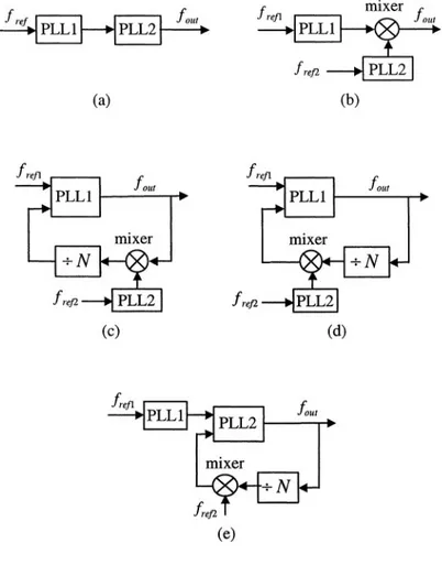
C. Multi-loop PLL-FS
Figure 2-11. Dual-loop PLL frequency synthesizers
2.3.4 DLL-based frequency synthesizer
Figure 2-12. Block diagram of DLL-FS
2.3.5 Hybrid frequency synthesizer
Many systems incorporate a mixture or hybrid of these basic approaches in order to take advantage of the benefits of increased speed or improved resolution that one approach may have over another. For example, sometimes a PLL synthesizer may incorporate a DDS in its reference circuitry to increase resolution or to reduce switching time [47]. A major drawback of this approach is that the PLL acts as a multiplier on any phase noise or spurs in its reference and a DDS may have high spurs. The resulting noise at PLL output can seriously degrade system performance.
2.3.6 Summary and comparison of synthesizers
The most widely used frequency synthesizer architecture is based on PLL. It can be easily integrated in current technologies, consumes reasonable power, and meets most of the wireless and wired RF applications. The
2.4
Frequency synthesizer for wireless transceivers
Frequency synthesizers are used as local oscillators (LO) in the wireless transceivers for frequency translation and channel selection. Figure 2-13 shows the popular super-heterodyne receiver architecture [1]. It is a two-step down-conversion architecture. A tunable RF LO is for both the first step frequency conversion and channel selection, and an IF fixed-frequency LO is for further frequency down-conversion to baseband.
Figure 2-13. Super-heterodyne receiver architecture
Figure 2-14. GSM base station receiver architecture
Figure 2-14 illustrates a typical low-IF (10.7MHz) architecture for a GSM base-station receiver. In this architecture the FS for LO1 is tunable between 640MHz to 675MHz. For a reference frequency of 200kHz, the PLL divide ratio varies between 3200 and 3375.
The signal mixing is actually a frequency convolution shown in Fig. 2-15. Suppose an incoming RF signal has a block signal level of
And the total noise in a channel of bandwidth (dBHz) due to this undesired down-conversion is
With the received RF signal power of the down-converted IF signal
power is
Thus, the signal-to-noise ratio (SNR) after down-conversion is
Therefore, for the minimum received signal level of the
maximum block signal level of and the minimum required SNR,
the phase noise requirement can be calculated as [49]:
Figure 2-15. Down-conversion with phase noise
For example, in the GSM standard the minimal received signal (sensitivity) is –120dBm, the maximum interference power level from 600kHz to 1.6MHz offset is –43dBm, the channel bandwidth is 200kHz, and the required SNR is 9dB. According to (2.31) and (2.32), in this offset frequency range, the phase noise and spur level should be less than
–121dBc/Hz and –68dBc, respectively. Another example is the derivation of phase noise requirement for Bluetooth receiver at 3MHz offset. The out-of-band interference power beyond 3MHz offset is –40dBm, the channel bandwidth is 1MHz, the required SNR is 16dB, and the block margin at 3MHz is 6dB. If we want to achieve an input sensitivity of –82dBm (better than the specified –70dBm), the phase noise at 3MHz should be less that
–124dBc/Hz.
2.5
Other applications of PLL and frequency synthesizer
if leads the VCO control voltage reduces. Thus it causes the VCO output frequency and phase to reduce.
The basic PLL finds its application in clock de-skew for high-speed digital and mixed-signal IC’s, clock synthesis, carrier recovery, clock recovery, modulation and demodulation of frequency or phase [50], and filter tuning [51], [52].
Figure 2-16. Basic PLL diagram
Figure 2-17. PLL for frequency demodulation
Figure 2-18. PLL for phase demodulation
output frequency tracks the input carrier frequency and is the average of
As shown before (see Figs. 2-7 and 2-10), with a frequency divider added between VCO and PD, the PLL’s output frequency can be either an integer or a fractional times of the reference frequency. Like basic PLL’s, frequency synthesizers are widely used in electrical engineering. It applications include frequency translation and channel selection in wireless and broadband communications, clock and data recovery in receivers, frequency or phase modulation and demodulation, detection in radar systems, special purpose instruments, and on-chip clock generation and synchronization for digital and mixed-signal IC’s, etc.
The clock and data-recovery (CDR) based on PLL is to synchronize the random data to a clock signal generated by a VCO in the PLL. Quadricorrelator shown in Fig. 2-19 is a good technique to implement the reference-less frequency detection [53], [54].
Figure 2-19. Simplified quadricorrelator CDR architecture
REFERENCES
[1] [2] [3] [4]
A. Zanchi, C. Samori, S. Levantino, and A. Lacaita, “A 2-V 2.5-GHz-104-dBc/Hz at 100 kHz fully integrated VCO with wide-band low-noise automatic amplitude control loop,” IEEE J. Solid-State Circuits, vol. 36, pp. 611-619, Apr. 2001
A. Zanchi, C. Samori, A. Lacaita, and S. Levantino, “Impact of AAC design on phase noise performance of VCOs,” IEEE Trans. Circuits Syst. II, vol. 48, pp. 537-547, June 2001
L. Lin, “Design techniques for high performance integrated frequency synthesizers for multi-standard wireless communication applications,” Ph.D. dissertation, University of California at Berkeley, CA, Dec. 2000
F. Herzel and B. Razavi, “A study of oscillator jitter due to supply and substrate noise,”
[5]
J. McNeill, “Jitter in ring oscillators,” IEEE J. Solid-State Circuits, vol. 32, pp. 870-879, June 1997
T. Lee and A. Hajimiri, The Design of Low Noise Oscillators. Boston, MA: Kluwer, 1999
A. Hajimiri, “Noise in phase-locked loops,” in Proc. Southwest Symp. Mixed-Signal Design (SSMSD), Feb. 2001, pp. 1-6
L. Dai and R. Harjani, Design of High Performance CMOS Voltage-Controlled Oscillators. Boston, MA: Kluwer, 2003
B. Kim, T. Weigandt, and P. Gray, “PLL/DLL system noise analysis for low jitter clock synthesizer design,” in Proc. IEEE Int. Symp. Circuits and Systems (ISCAS), vol. 4, London, UK, May 1994, pp. 31-34
A. Demir, A. Mehrotra, and J. Roychowdhury, “Phase noise in oscillators: a unifying theory and numerical methods for characterization,” IEEE Trans. Circuits Syst. I, vol. 47, pp. 655-674, May 2000
L. Dai, “Design of high-performance VCOs for communications,” Ph.D. dissertation, The University of Minnesota, Ann Arbor, MI, 2002
C. Samori, A. Lacaita, A. Zanchi, and F. Pizzolato, “Experimental verification of the link between timing jitter and phase noise,” Electronic Letters, vol. 34, pp. 2024-2025, Oct. 1998
A. Demir, A. Mehrotra, and J. Roychowdhury, “Phase noise and timing jitter in oscillators,” in Proc. CICC’98, May 1998, pp. 45-48
B. Drakhlis, “Calculate oscillator jitter by using phase-noise analysis,” Microwave & RF, pp. 82-90, 157, Jan. 2001
J. McNeill, “A simple method for relating time- and frequency-domain measures of oscillator performance,” in Proc. SSMSD’2001, Feb. 2001, pp. 7-12
U. Moon, K. Mayaram, and J. Stonick, “Spectral analysis of time-domain phase jitter measurements,” IEEE Trans. Circuits Syst. II, vol. 49, pp. 321-327, May 2002
A. Zanchi, A. Bonfanti, S. Levantino, and C. Samori, “General SSCR vs. cycle-to-cycle jitter relationship with application to phase noise in PLL,” in Proc. SSMSD’2001, Feb. 2001, pp. 32-37
J. Yang, S. Kim, S. Kim, and B. Jeon, “Fast switching frequency synthesizer using direct analog techniques for phase-array radar,” Radar 97, Oct. 1997, pp. 386-390 A. Rokita, “Direct analog synthesis modules for an X-band frequency source,”
International Conference on Microwaves and Radar, vol. 1, May 1998, pp. 63-68 W. Egan, Frequency Synthesis by Phase Lock. John Wiley & Sons, 2000
V. Reinhardt, “Spur reduction techniques in direct digital synthesizers,” in Proc. Int. Frequency Control Symp., June 1993, pp. 230-241
H. Wolfson, “Very small frequency generator systems for spread spectrum EHF applications,” MILCOM’89, vol. 3, Oct. 1989, pp. 749-753
J. Nieznanski, “An alternative approach to the ROM-less direct digital synthesis,” IEEE J. Solid-State Circuits, vol. 33, pp. 169-170, Jan. 1998
A. Yamagishi, M. Ishikawa, T. Tsuneo, and S. Date, “A 2-V, 2-GHz low-power direct digital frequency synthesizer chip-set for wireless communication,” IEEE J. Solid-State Circuits, vol. 33, pp. 210-217, Feb. 1998
A. Madisetti, A. Kwentus, and A. Willson, “A 100-MHz, 16-b, direct digital frequency synthesizer with 100-dBc spurious-free dynamic range,” IEEE J. Solid-State Circuits,
vol. 34, pp. 1034-1043, Aug. 1999
S. Mortezapour and E. Lee, “Design of low-power ROM-less direct digital frequency synthesizer using nonlinear digital-to-analog converter,” IEEE J. Solid-State Circuits,
[27]
A. Bellaouar, M. O’Brecht, A. Fahim, and M. Elmasry, “Low-power direct digital frequency synthesis for wireless communications,” IEEE J. Solid-State Circuits, vol. 35, pp. 385-390, Mar. 2000
A. Sodagar and G. Lahiji, “Mapping from phase to sine-amplitude in direct digital frequency synthesizers using parabolic approximation,” IEEE Trans. Circuits Syst. II,
vol. 47, pp. 1452-1457, Dec. 2000
D. Calbaza and Y. Savaria, “Direct digital frequency synthesis of low-jitter clocks,”
IEEE J. Solid-State Circuits, vol. 36, pp. 570-572, Mar. 2001
S. Liu, T. Yu, and H. Tsao, “Pipeline direct digital frequency synthesizer using decomposition method,” IEE Proc. Circuits Devices Syst, vol. 48, June 2001
A. Sodagar and G. Lahiji, “A pipelined ROM-less architecture for sine-output direct digital frequency synthesizers using the second-order parabolic approximation,” IEEE Trans. Circuits Syst. II, vol. 48, pp. 850-857, Sept. 2001
J. Jiang and E. Lee, “A low-power segmented nonlinear DAC-based direct digital frequency synthesizer,” IEEE J. Solid-State Circuits, vol. 37, pp. 1326-1329, Oct. 2002 A. Mohieldin, A. Emira, and E. Sánchez-Sinencio, “A 100-MHz 8-mW ROM-less quadrature direct digital frequency synthesizer,” IEEE J. Solid-State Circuits, vol. 37, pp. 1235-1243, Oct. 2002
D. Wilson, R. Woogeun, and B. Song, “Integrated RF receiver front ends and frequency synthesizers for wireless,” Designing Low Power Digital Systems, Emerging Technologies (1996), 1996, pp. 369-396
U. Rohde, “Synthesizer design for microwave applications,” http://www. synergymwave.com
C. Park, O. Kim, and B. Kim, “A 1.8GHz self-calibrated phase-locked loop with precise I/Q matching,” IEEE J. Solid-State Circuits, vol. 36, pp. 777-783, May 2001
K. Lee, “A single-chip 2.4GHz direct-conversion CMOS receiver for wireless local loop using multiphase reduce frequency conversion technique,” IEEE J. Solid-State Circuits, vol. 36, pp. 800-809, May 2001
C. Heng and B. Song, “A l.8GHz CMOS fractional-N frequency synthesizer with randomized multi-phase VCO,” in Proc. IEEE 2002 Custom Integrated Circuits Conf. (CICC), May 2002, pp. 427-430
B. Miller and B. Conley, “A multiple modulator fractional divider,” Proc. Annu. Frequency Control Symp., May 1990, pp. 559-568
B. Miller and R. Conley, “A multiple modulator fractional divider,” IEEE Trans. Instrumentation and Measurement, vol. 40, pp. 578-583, June 1991
T. Riley, M. Copeland, and T. Kwasniewski, “Delta-sigma modulation in fractional-N frequency synthesis,” IEEE J. Solid-State Circuits, vol. 28, pp. 553-559, May 1993 W. Yan and H. Luong, “A 2-V 900-MHz monolithic CMOS dual-loop frequency synthesizer for GSM receivers,” IEEE J. Solid-State Circuits, vol. 36, pp. 204-216, Feb. 2001
T. Kan, G. Leung, and H. Luong, “2-V, 1.8-GHz fully integrated CMOS dual-loop frequency synthesizer,” IEEE J. Solid-State Circuits, vol. 37, pp. 1012-1020, Aug. 2002 T. Aytur and J. Khoury, “Advantages of dual-loop frequency synthesizers for GSM applications,” in Proc. IEEE ISCAS’97, vol. 1, Hong Kong, June 1997, pp. 17-20 G. Chien and P. Gray, “A 900MHz local oscillator using a DLL-based frequency multiplier for PCS applications,” IEEE J. Solid-State Circuits, vol. 35, pp. 1996-1999, Dec. 2000
[47]
A. Rofougaran, G. Chang, J. Rael, J. Chang, M. Rofougaran, P. Chang, M. Djafari, M. Ku, E. Roth, A. Abidi, and H. Samueli, “A single-chip 900-MHz spread-spectrum wireless transceiver in CMOS - part I: architecture and transmitter design,” IEEE J. Solid-State Circuits, vol. 33, pp. 515-534, Apr. 1998
J. Rudell, J. Ou, R. Narayanaswami, G. Chien, J. Weldon, L. Lin, K. Tsai, L. Lee, K. Khoo, D. Au, T. Robinson, D. Gerna, M. Otsuka, and P. Gray, “Recent developments in high integration multi-standard CMOS transceivers for personal communication systems,” in Proc. Int. Symp. Law Power Electronics and Design, Monterey, CA, Aug. 1998, pp. 149-154
C. Lo, “A 1.5-V 900-MHz Monolithic CMOS fast-switching frequency synthesizer for wireless applications,” Master thesis, The Hong Kong University of Science and Technology (HKUST), China, Jan. 2000
D. Wolaver, Phase-locked Loop Circuit Design. New Jersey: Prentice Hall, 1991 D. Li, “Theory and design of active LC filters on silicon,” Ph.D. dissertation, Columbia University, New York, May 2000
H. Liu and A. Karsilayan, “An automatic tuning scheme for high-frequency bandpass filters,” in Proc. IEEE ISCAS, vol. 3, Phoenix, AZ, May 2002, pp. 551-554
J. Savoj and B. Razavi, High-speed CMOS Circuits for Optical Receivers. Boston, MA: Kluwer, 2001
PLL FREQUENCY SYNTHESIZER
This chapter presents the analysis of PLL-based frequency synthesizers. It includes the continuous-time linear analysis, discrete-time analysis, operation modes, stability, and fast-locking techniques. An integer-N PLL synthesizer design example is given to illustrate the system-level parameter design procedure.
3.1
PLL frequency synthesizer basics
3.1.1 Basic building blocks of charge-pump PLL
The block diagram of the PLL frequency synthesizer is shown in Fig. 3-1. It is based on a charge-pump PLL [1] and consists of a phase-frequency detector (PFD), a charge-pump (CP), a loop filter (LF), a voltage-controlled oscillator (VCO), a dual-modulus prescaler, and a programmable pulse-swallowing divider. The divide ratio of the dual-modulus prescaler is P or
P+1. M and A are programmable integers [2], [3]. Each divider output cycle consists of (P+1)·A+P·(M–A) VCO cycles. Thus the nominal frequency divide ratio is:
Figure 3-1. Charge-pump PLL frequency synthesizer
Figure 3-2. Tri-state phase-frequency detector (PFD)
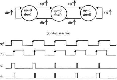
The phase detector (PD) detects the phase difference between the reference signal and the feedback signal from the VCO and frequency divider. Note that, although the PD of a PLL can be an analog multiplier, an exclusive-or (XOR) gate or a J-K flip-flop, etc, for a frequency synthesizer we always use the charge-pump PLL with a tri-state phase-frequency detector (PFD) that also detects frequency errors [3]. Note that, this tri-state PFD is also referred to as “type-4” PD in the literature. The charge-pump PLL has two poles at the origin (type-II) in its open-loop transfer function. It locks faster and its static phase error is zero if mismatches and leakages are negligible. Moreover, its capture range is only limited by its VCO tuning range. A PFD is usually built with memory elements such as flip-flops, latches, etc. Figure 3-2 shows a widely used PFD based on two flip-flops. This edge-triggered tri-state PFD has a linear phase detection range of radians. It is duty-cycle insensitive. The delay in the reset path is used to eliminate the dead zone (undetectable phase difference range).
The functionality of the PFD is depicted by its state machine diagram, and waveforms of its inputs and outputs shown in Fig. 3-3. When the rising edge of the reference inputref leads that of the divided VCO feedback input
capacitors in the loop filter. Thus, the loop filter output voltage increases and so do the VCO output frequency and phase.
The charge-pump transfers phase difference into current. Fig. 3-4 shows the principles of charge-pump and loop filter. The charge-pump converts the
up and dn pulses into current pulses and these current pulses change voltage drop on the loop filter impedance is also the VCO control voltage. The dual-modulus prescaler is a high-speed frequency divider to bridge the gap between the low-speed programmable divider and the high frequency (e.g. a few GHz) VCO. The quantitative analysis of reference spurs due to charge-pump nonidealities in [4] is reexamined in Chapter 7.
Figure 3-3. Functionality of PFD
The transfer characteristic from the phase error at PFD input to the average charge-pump output current per reference period is shown in Fig. 3-5. It indicates that the PFD has a linear input range of
Figure 3-5. PFD/CP transfer function characteristic
3.1.2 Continuous-time linear phase analysis
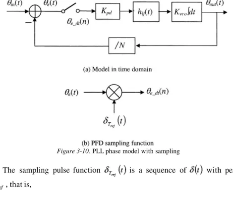
Since PLL’s used for frequency synthesizers are unanimously charge-pump PLL (CP-PLL). Here all analyses are based on this type of PLL. Figure 3-6 gives the linear phase (noise) analysis model of charge-pump PLL. The PFD and charge-pump are combined as one block. Phase noise generated by each building block is referred to its output.
Figure 3-6. PLL linear phase noise model
input phase noise, mainly from the reference signal current noise associated with PFD and charge pump voltage noise generated by loop filter
VCO output phase noise PLL output phase noise
phase noise generated by the frequency divider (including prescaler)
gain of PFD and charge pump, which is is the CP
current
N: frequency division ratio
Disconnecting the feedback loop between the divider and PFD, we define the PLL open-loop phase transfer function as:
The transfer function for each noise source to the output phase noise is listed in Table 3-1.
From Table 3-1, we know that the input noise and divider noise have the same transfer function magnitude to the PLL output.
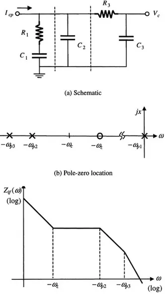
Figure 3-7. Passive loop filter for charge-pump PLL
where
is the zero in the loop filter for loop stability. The pole is located in the origin, i.e., The PLL open-loop (disconnecting the divider and PFD) gain is:
where the PLL loop gain is:
Thus the crossover frequency, where the open-loop gain is unity, is solved from
or simply
where the phase margin is:
Thus, the damping factor and natural frequency are as follows:
Equation (3.11) yields:
From (3.14) we know that the closed loop gain has a low-pass characteristic. It is equal to the frequency divide ratio N when or
It is reduced by 3dB at
Table 3-2 lists the relationship between ratio and the damping factor
Note that and as in this book we refer to the PLL open-loop
unity gain frequency as the PLL bandwidth.
Figure 3-8. Natural frequency and damping factor vs. phase margin
For the second-order passive loop filter (with and in Fig. 3-7 (a)), the transimpedance is
where and the second pole is:
The open-loop gain is
where and The open-loop phase-margin is:
For maximum phase margin, we have
Therefore, the optimal phase margin is
Thus, the maximum phase margin is exclusively determined by the
capacitor ratio b . In the meantime, and the PLL
bandwidth in (3.19) is simplified as:
In a real PLL, the inaccuracy of resistance and capacitance of an on-chip loop filter and variance of VCO conversion gain affects the phase margin. The variation of resistance and capacitance is typically 10%~20%, while the variation of can be more than a factor of 2. Therefore, we have to keep enough phase-margin to accommodate variations of design parameters. Figure 3-9 illustrates the PLL phase margin for different values from 5 to 30, when deviates from its optimal value of
It shows that the phase margin is not much sensitive to the
variation of and ratio. For example, in case of
the optimal phase margin is 55°, and it degrades to 48.7° when deviates
from its optimal value by a factor of 2, i.e.,
The closed-loop phase (noise) transfer function of charge-pump PLL with second-order passive loop filter is:
When the loop bandwidth is chosen for maximum phase margin (see 3.21), (3.24) can be written as
Equation (3.25) can be rewritten as:
where the damping factor and natural frequency are as follows.
When (i.e., b = 9), in (3.26) has three poles at the loop bandwidth and one zero at one-third of as shown in (3.30).
For the third-order passive loop filter (see Fig. 3-7 (a)), the transimpedance is
Usually, and
Therefore, the two non-zero poles are as follows.
where The open-loop phase-margin is:
Usually, the phase-margin degradation due to the third pole
is very small, the maximum still occurs around Since
the PLL bandwidth in (3.35) is simplified as:
More discussions on high-order loop filter design can be found in the literature [5]-[9]. For example, the exact relationship among
and in the fourth-order PLL for maximum is derived in [9].
Note that the above phase-margin calculation is based on the continuous-time linear model of the charge-pump PLL. This model is good for loop bandwidth less than 1/10 of the reference frequency Otherwise the
settling behavior will differ from the calculations significantly. With the loop delay taken into account, the PLL open-loop gain and phase margin become:
Therefore, the loop delay degrades the phase margin, and hence reduces the damping factor [10]. Usually, the loop delay is small and the phase margin degradation is negligible. In [11], the PLL sampling delay due to discrete-time operation of PFD is modeled as the PFD update period
Figure 3-10. PLL phase model with sampling
The sampling pulse function is a sequence of with period
that is,
3.1.3 Locking time
Considering that the PLL is initially locked and the frequency divide ratio changes due to channel switching, we calculate the locking time for a given frequency error. Locking time is also referred to as settling time or switching time.
where
and Note that the two non-zero poles of are
unequal real numbers because
Equation (3.42) leads to the following PLL closed-loop phase or frequency transfer function:
For simplicity, we ignore these high order terms, which are smaller than lower order terms. The consequences of this simplification are more on the initial characteristics, such as overshoot, and less on long time behavior, such as lock time. The simplified second-order expression is:
Defining the damping factor and natural frequency:
Thus, the two poles of the second-order transfer function are:
When the PLL output frequency changes from to due to the change of N, it is equivalent to change the reference frequency from to Note that, the value of N used in all of these equations should be the value corresponding to the new output frequency This approximation does not cause much error when the change in the value of N is relatively small and the instantaneous phase error is less than The lock time can be readily evaluated by means of the final value theorem of the Laplace transformation, which states that:
The PLL output frequency responds to the input frequency step as:
Equation (3.52) is plotted in Fig. 3-11 (a). The normalized time for x-axis
is It is under-damped for critical-damped for and
over-damped for
To check the error introduced by the approximation in (3.45), the exact for the third-order charge-pump PLL is derived in (3.53) using
in (3.29) and (3.30). Note that, the damping factor and natural frequency in (3.53) are those defined for the third-order PLL in (3.27) and (3.28), respectively.
As illustrated in Fig. 3-11 (b), we see the discrepancy between the settling behavior of the second- and the third-order PLL’s. Although it is difficult to derive the exact for the fourth-order PLL, its difference from that of the third-order one is negligible because the third pole of the loop filter is usually more than one order larger than the PLL bandwidth
Figure 3-12 illustrates the PLL output frequency-settling behavior for a relative frequency error of For example, from this figure we read that for damping factor the settling time, which is normalized by a
factor of is about 14 and 17 for the second and third-order PLL, respectively. Figure 3-13 (a) gives the MATLAB simulated normalized
settling time for and and For
Figure 3-13. PLL locking time (continued)
Approximate formulas to calculate the settling time in the literature are mostly based on (3.52), which is accurate for the second-order PLL. For most design, and the term in the brackets of (3.52) has a
maximum value of therefore the locking time is [3], [12]:
where the specified frequency accuracy is:
The locking time formula of the third-order PLL based on transient simulations given in [13] is:
where is defined as an effective damping factor depending on phase margin Reference [13] only gives the average for
obtained from transient simulations. Based on behavioral-level simulation, the discrete-time effect on the third-order PLL locking time is also provided in [13], which shows that the increase of PLL locking time due to PFD delay is relatively small.
The locking time formula for a simple first-order PLL derived in [14] is:
and the formula for the second-order PLL given in [15] is:
Further simplified [16] locking time expression is:
Note that the above locking time calculations are based on the linear continuous-time model of the charge-pump PLL. This model is good for loop bandwidth much less than 1/10 of the reference frequency
Otherwise the settling behavior will deviate from the calculations substantially as shown in [17].
Moreover, to check if the maximum phase error during the settling is in the linear PFD range of we calculate the maximum PFD phase error during the transient response to a frequency step input.
Therefore, the instantaneous PFD phase error for a frequency step input is
Given the expression of the second and third order PLL in (3.48) (or (3.14)) and (3.25), respectively, the inverse Laplace transformation gives the transient phase error in time domain as
The normalized PFD phase error, is plotted in Fig.
value of 0.45 (or 0.85) for the second (or third) order PLL. Fig. 3-14 (b) reveals that to keep the phase error in the range of for a third-order PLL, the input referred frequency step, should be in the range of A similar result based on transient simulations of a third-order PLL is given in [17] as:
Finally, if the overload of charge pump or VCO occurs due to under-damped overshoot, the locking time will be longer. We can calculate the overshoot to check if overload occurs. The transfer function of the input phase to the VCO control voltage in a charge-pump PLL is
where is the VCO control voltage corresponding to output frequency When the VCO output frequency changes from to the transient response of VCO control voltage change is
Using inverse Laplace transformation, it yields
where for the second or third-order PLL is given in (3.52) or (3.53). The normalized control voltage change is plotted in Fig. 3-15. Overshoot increases when damping factor decreases. For example, when
the overshoot is about 20% and 30% of the control voltage change for the second and third order PLL’s, respectively.
3.1.4 Tracking and acquisition
Tracking is the transient response of a PLL output to
phase in the locked state, and acquisition is the process of bringing an the change of input
unlocked loop into lock. Although the tracking or acquisition process was originally defined for a PLL with analog multiplier PD, it can be extended to the charge-pump PLL frequency synthesizers. The four PLL operation ranges are as follows:
(1)
(2)
(3)
The hold range is the frequency range in which PLL operation can be statistically stable. For charge-pump PLL, Thus, the actual hold range is only restricted by the PLL tuning range.
The lock range by definition is the frequency offset between the inputs of analog multiplier PD, which causes the PLL to acquire lock in one beat note for linear PLL. For charge-pump PLL,
Since the lock-in process is roughly completed within one cycle of the
damped oscillation, the lock-in time
the pull-in process. Thus the pull-in time is
(4) The pull-out range is the size of the frequency step applied to the reference input which causes the PLL to lose phase tracking. Because the PFD output is linear in the range of it can be computed explicitly using the linear model.
The least-square fit gives the linear approximation [18]:
The operating ranges of a second-order charge-pump PLL are summarized in Table 3-3.
For PLL’s with other types of phase detector, such as the analog multiplier, XOR gate and JK flip-flop, the formulas of their operating ranges can be found in [18].
and the
3.2
Fast-locking techniques
Fast locking in frequency synthesizer is required for modern communication systems, such as digital cellular mobile systems [19], car radio receivers [13] and frequency-hopped (FH) systems [20]. Since for a charge-pump PLL, the locking time is inversely proportional to the loop bandwidth, the locking time might be longer than a specific requirement for a given loop bandwidth. For example, for the frequency synthesizer in [13], the SNR constraint asks for 800Hz bandwidth, but the settling times requires at least 3.2kHz bandwidth. Thus various techniques have been used to achieve fast PLL locking after the channel switching. Basically, these techniques are divided into two categories: speed-up mode and VCO pre-tuning.
3.2.1 Bandwidth gear-shifting
The basic idea behind this scheme is gear-shifting, that is, using a larger loop bandwidth during the frequency switching transition and shifting the loop bandwidth to the normal value after the PLL is locked or after a certain (programmable) period of time.
One speed-up mode is to use both proportional and integral charge-pump currents, as shown in Fig. 3-16. The loop filter output voltage in the speed-up mode is: