Formation of Palladium Silicide Thin Layers on Si(110) Substrates
Risa Suryana
, Osamu Nakatsuka, and Shigeaki Zaima
Department of Crystalline Materials Science, Graduate School of Engineering, Nagoya University, Nagoya 464-8603, Japan
Received November 13, 2010; accepted February 20, 2011; published online May 20, 2011
The formation of palladium silicide thin films from Pd/Si(110) and Pd/Si(001) systems with and without a Ti intermediate layer has been investigated. The existence of a Ti layer could improve the thermal stability of Pd2Si thin layers in Pd/Ti/Si(001). In addition, an epitaxial or highly oriented Pd2Si layer is formed in Pd/Ti/Si systems. However, the roughness of the Pd2Si/Si interface is observed in Pd/Ti/Si(110) systems, while the flatnesses of the Pd2Si/Si interface is observed in Pd/Ti/Si(001). #2011 The Japan Society of Applied Physics
1. Introduction
Three-dimensional (3D) devices, such as fin-field-effect transistors (Fin-FET), are one of the promising candidates to replace classical planar metal–oxide–semiconductor field-effect transistors (MOSFETs) for future complementary metal–oxide–semiconductor (CMOS) technologies due to the multigate configuration of the FET device leading to an intrinsically superior short-channel effect (SCE) control.1–4)
A major concern for Fin-FETs is the increase in the parasitic source-drain resistance (Rsd) as the fin width is scaled. As fins must be narrow in order to control SCEs, the reduction in Rsd is a critical issue. It has been reported that one of methods to reduce theRsd is the source/drain (S/D) contact configuration of the Fin-FET structure.4,5)Okuyama et al.5) have calculated the drain current–gate voltage (ID–VG) characteristics of Fin-FETs with top and wrapped contact configurations. They concluded that the Rsd causes a driving-current decrease for the top contact configuration compared with the wrapped contact configuration.
Considering the Fin-FET configuration as mentioned in refs.4 and 5, the electron mobility in the channel on a Si(001) surface and the hole mobility in the channel on a Si(110) surface are the largest among those observed for various surface orientations,6,7)one way to implement these
two different crystal orientations is to align silicon fins to be parallel to the (001) orientation for NMOS or parallel to the (110) orientation for PMOS on a Si(110) wafer. Therefore, in the S/D wrapped contact configuration, we have to consider the interfaces between metal silicides and the silicon surface, i.e., (110) and (001) interfaces, in order to increase the Fin-FET performance.
Here, palladium (Pd) silicide is potentially attractive from the viewpoint of contact materials for ultrathin silicide films on shallow junctions because Pd forms a metal-rich silicide, Pd2Si,8,9) which remains stable up to 700C after the
formation at a low temperature, and the consumption of Si for the Pd2Si formation is smaller than those of conventional
silicides, such as NiSi, CoSi2, and TiSi2.10) However, the
agglomeration of Pd2Si has been a serious problem that
results in the degradation of metal contact (S/D) perfor-mance in MOSFET applications. We previously reported that Pd2Si agglomeration occurs at temperatures of 550–
600C in Pd/Si(001) systems.11,12)
In general, an epitaxial layer is defined as the growth of a single-crystal overlayer on the surface of a single-crystal substrate. Using this definition, epitaxy is typically limited to homointerfaces (e.g., Si on Si) or heterointerfaces with similar crystallographic structures and lattice constants (e.g., SiGe on Si). Nevertheless, materials with dissimilar crystal-lographic structures may also grow in a distinctively ordered way on the surface of a single-crystal substrate. Thus, in this paper, the term ‘‘epitaxial’’ is used to describe the preferential orientation of the grains within such textured layers. It should be noted that several types of epitaxially matching grains may coexist within the same layer.
Previously, we reported that epitaxial or highly oriented Pd2Si layers can be formed on a Si(001) substrate using a Ti
intermediate layer with and without heavy B-doping at annealing temperatures of 300–600C.12)
In addition, the agglomeration of Pd2Si in Pd/Ti/Si(001) can be suppressed
with the epitaxial growth of Pd2Si layers at 600C with and
without heavy B-doping. The flatnesses of the Pd2Si/Si(001)
interface were similar with and without heavy B-doping. It seems that the doping of boron atoms on a Si substrate in a Pd/Ti/Si(001) system does not significantly affect the epitaxial Pd2Si formation. Hoffman et al.13) reported that
heteroepitaxial Pd2Si can be formed by the predeposition of
a Ti intermediate layer (0.1–1.5 nm) prior to the deposition of Pd (3 nm) on Si(001) and Si(111) at 250C. To our knowledge, no one has reported the formation of Pd2Si using
a Ti intermediate layer on a Si(110) substrate. Considering the formation of wrapped contacts for Fin-FET structures on Si(110) substrates, it is necessary to clarify the properties of Pd silicide thin layers on a Si(110) surface. In this study, we investigated the growth and thermal stability of Pd silicide thin films on Si(110) substrates with and without a Ti intermediate layer.
2. Experimental Methods
The substrates used were n-type Si(110) wafers with a resistivity of 1–2cm. After the standard acid treatment, the wafers were dipped into a diluted HF solution and rinsed for 5 s in deionized water in order to remove the surface oxide and to obtain H-passivated surfaces.14) Immediately, the wafers were loaded into a ultrahigh-vacuum (UHV) chamber.
10-nm-thick Pd and 2-nm-thick Ti layers followed by a 10-nm-thick Pd layer were formed on the substrates by electron gun evaporation in a UHV chamber whose base pressure was below 110 6
Pa. Hereafter, these samples were called Pd/Si(110) or Pd/Ti/Si(110) samples, respec-tively. The samples were successively annealed at 300C in Present address: Physics Department, Faculty of Mathematics and Natural
Sciences, Sebelas Maret University, Jl. Ir. Sutami 36A Kentingan Surakarta 57126, Indonesia. E-mail address: [email protected]. ac.jp
the same chamber for 10 min, and then, they were exposed to atmosphere. Some samples were additionally annealed at temperatures ranging from 400 to 600C for 30 s in N
2
ambient using a rapid thermal annealing (RTA) system. X-ray diffraction (XRD) analysis using a Cu Ksource, cross-sectional transmission electron microscopy (XTEM), and scanning electron microscopy (SEM) were performed to determine the crystalline structures and morphologies of the films. For comparison, we also present the experimental data of Pd/Si(001) and Pd/Ti/Si(001) systems, which have similar experimental conditions to Pd/Si(110) and Pd/Ti/ Si(110) systems.
3. Results and Discussion
Figure 1 shows the XRD 2 spectra of Pd/Si(110) and Pd/Si(001) samples without a Ti intermediate layer after annealing at 300C for 10 min and the additional RTA at 400–600C for 30 s. Similar diffraction peaks related to Pd2Si are observed in both Pd/Si(110) and Pd/Si(001)
samples regardless of the annealing temperature. However, the intensities of these peaks at the same peak position between the Pd/Si(110) and Pd/Si(001) samples are different. Two major diffraction peaks at about 38.10 and 53.70 are identified as Pd
2Si 111 and 002, respectively.
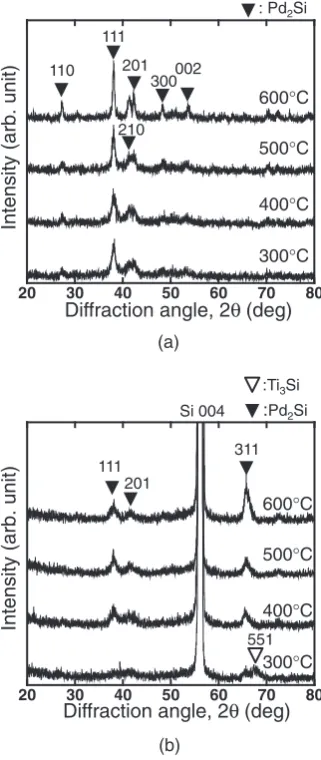
Figure 2 shows the XRD2spectra of Pd/Ti/Si(110) and Pd/Ti/Si(001) samples after annealing at 300C for 10 min and the additional RTA at 400–600C for 30 s. In contrast to the Pd/Si systems, the peaks of Pd2Si in the Pd/Ti/
Si systems are weaker and not many. The major Pd2Si
peak is only 111 at about 38.10 in the Pd/Ti/Si(110) samples and 311 at about 65.83 in the Pd/Ti/Si(001) samples.
We performed XRD2=!spectral analysis to determine why the peaks of Pd2Si in the Pd/Ti/Si systems weaken,
which is likely caused by the formation of an epitaxial or highly oriented Pd2Si layer. The XRD2=!spectra clearly
revealed that an epitaxial or highly oriented Pd2Si layer is
formed in Pd/Ti/Si samples after annealing at 300–600C, as shown in Fig. 3. Only the highly oriented Pd2Si 111 is
formed in Pd/Ti/Si(110) samples, while the highly oriented Pd2Si 110 and PdSi 211 are formed in Pd/Ti/Si(001)
samples. These peaks do not appear on the samples without a Ti layer (not shown). It is considered that a Ti intermediate layer controls the interfacial reaction for the formation of an epitaxial or highly oriented Pd2Si layer.
The grain size of Pd2Si crystallites for each orientation
sample can be estimated from the diffraction profiles by using the following Scherrer formula:15)
20 30 40 50 60 70 80
101 111
201 002
112 212302
Diffraction angle, 2θ (deg)
Intensity (arb. unit)
:Pd2Si
300°C 400°C 500°C 600°C
(a)
20 30 40 50 60 70 80
300°C 400°C 500°C
600°C
Diffraction angle, 2θ (deg)
Intensity (arb. unit)
Si 004 : Pd2Si
101 111
201 002
112 212 302
(b)
Fig. 1. XRD (2) profiles of the (a) Pd (10 nm)/Si(110) and (b) Pd (10 nm)/Si(001) systems without Ti interlayer after annealing at 300– 600C.
20 30 40 50 60 70 80
Diffraction angle, 2θ (deg)
Intensity (arb. unit)
110 201
111
210 300002
300°C 400°C 500°C 600°C
: Pd2Si
(a)
20 30 40 50 60 70 80
Diffraction angle, 2θ (deg)
Intensity (arb. unit)
300°C 400°C 500°C 600°C
111 201
311 Si 004
551
:Pd2Si :Ti3Si
(b)
B¼ K
tcos; ð1Þ
whereBis the grain size,is the wavelength of the X-ray,t is the full-width at half maximum (FWHM) of the diffraction peak, and is the Bragg angle. The correction factor K contains information about temperature, internal stress, and so forth, and its value is generally 0.9.16)These parameters are estimated by Gaussian fitting for a diffraction peak at a certain orientation in Figs. 1 and 2. On the basis of the shape and strength of the intensity profile, the grain size is calculated from the Pd2Si 111 and 002 lattice planes in the
Pd/Si systems and from the FWHM values of XRD peaks related to the Pd2Si 111 lattice plane for Pd/Ti/Si systems.
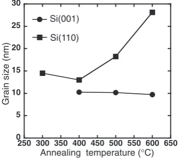
The dependences of Pd2Si grain size on the annealing
temperature in Pd/Si and Pd/Ti/Si samples are shown in Figs. 4 and 5, respectively. Figure 4 shows that the difference in grain size calculated from the FWHM values of XRD peaks related to Pd2Si for 111 and 002 lattice planes
is small for both Si(110) and Si(001) samples in the Pd/Si systems. The grain size of Pd2Si slightly increases with
annealing temperature in Pd/Si(110) and Pd/Si(001) samples. On the other hand, Fig. 5 shows that grain sizes
related to Pd2Si for 111 lattice planes increase after
annealing at 400C for the Pd/Ti/Si(110) samples. In contrast, these grain sizes are almost similar after annealing at 400C for the Pd/Ti/Si(001) samples. These results indicate that the Pd2Si layers are formed during the first-step
annealing at 300C, and we consider that the growth rate of Pd2Si in Pd/Ti/Si(110) systems is markedly higher than that
of Pd2Si in Pd/Ti/Si(001) systems as annealing temperature
increases during the second-step RTA.
20 30 40 50 60 70 80 111 Si 220
Intensity (arb. unit)
Diffraction angle, 2θ (deg) 300°C 400°C 500°C 600°C : Pd2Si
(a)
20 30 40 50 60 70 80
Si 002 Si 004
110
211
111
: Pd2Si
: PdSi : Pd
Intensity (arb. unit)
Diffraction angle, 2θ (deg) 300°C 400°C 500°C 600°C
(b)
Fig. 3. XRD (2=!) profiles of the (a) Pd (10 nm)/Si(110) and (b) Pd (10 nm)/Si(110) systems with Ti interlayer after annealing at 300–600C.
250 300 350 400 450 500 550 600 650 0
5 10 15 20 25 30
Annealing temperature (°C)
Grain size (nm)
Si(001)
Si(110)
(a)
250 300 350 400 450 500 550 600 650 0
5 10 15 20 25 30
Annealing temperature (°C)
Grain size (nm) Si(001)
Si(110)
(b)
Fig. 4. Grain sizes of (a) Pd2Si 111 and (b) Pd2Si 002 after annealing
from 300 to 600C in Pd (10 nm)/Si(110) and Pd (10 nm)/Si(001) systems.
0 5 10 15 20 25 30
250 300 350 400 450 500 550 600 650 Annealing temperature (°C)
Grain size (nm)
Si(001)
Si(110)
Fig. 5. Grain sizes of Pd2Si 111 after annealing from 300 to 600C in
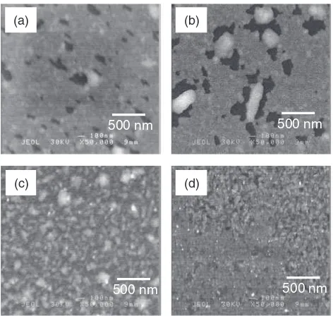
Figures 6(a) and 6(b) show SEM images of the Pd/ Si(110) and Pd/Si(001) samples, respectively, after anneal-ing at 600C for 30 s. The agglomeration of Pd
2Si layers and
the Si-exposed area corresponding to dark regions are clearly observed in both Pd/Si(110) and Pd/Si(001) samples. On the other hand, Si-exposed regions hardly appear in both Pd/Ti/Si(110) and Pd/Ti/Si(001) samples at 600C, as shown in Figs. 6(c) and 6(d). Nevertheless, the surface roughness of the Pd/Ti/Si(110) samples is more uneven than that of the Pd/Ti/Si(001) samples. It is considered that agglomeration is not suppressed by using a Ti intermediate layer in Pd/Ti/Si(110) systems, while it is suppressed by using a Ti intermediate layer in Pd/Ti/ Si(001) systems.
Figures 7(a)–7(d) show cross-sectional TEM images of the following samples after annealing at 600C: (a) the Pd/ Si(110), (b) Pd/Si(001), (c) Pd/Ti/Si(110), and (d) Pd/Ti/ Si(001) samples. A polycrystalline Pd2Si layer consisting of
domains with wedge-shape interfaces is clearly observed in Figs. 7(a) and 7(b) in the case without a Ti intermediate layer. Domains with facets are also observed in the Pd/Ti/
Si(110) sample, as shown in Fig. 7(c). In contrast, Fig. 7(d) shows a flat Pd2Si/Si interface in the Pd/Ti/Si(001) sample.
Considering that the dominant diffusion species during the formation of Pd and Ti silicides are Pd and Si, respec-tively,17,18) it is considered that, during annealing for silicidation, Pd atoms should diffuse into the Si substrate through a Ti intermediate layer to form an epitaxial Pd2Si
layer, and Si atoms should diffuse upward to form Ti silicides. Finally, the stacked layer structure consisting of a Ti silicide surface layer and a Pd2Si layer on a Si substrate is
formed.
Here, we deduced the model of the dependence of the interfacial reaction on annealing conditions. In general, a Pd2Si layer is formed by a diffusion-controlled process at
temperatures ranging from 100 to 700C.19)
In the case of annealing at a temperature of as low as 600C in Pd/Si systems, Pd atoms directly diffuse through Si and the Pd2Si
domain rapidly grows. As a result, Pd2Si grains easily
agglomerate either on Si(110) or Si(001) substrates. On the other hand, in the case of Pd/Ti/Si systems at a temperature of 600C, the diffusion of Pd atoms through a Ti intermediate layer is suppressed compared with that in the case of Pd/Si systems. The nucleation of epitaxial Pd2Si
simultaneously and densely occurs. Consequently, the uniform growth of a Pd2Si layer preferentially takes place,
i.e., the area of {100} facets decreases and a flat interface is formed. However, the Ti intermediate layer does not effectively retard the diffusion of palladium into the silicon in the Pd/Ti/Si(110) systems. This can be due to the growth rate of Pd2Si being higher on Si(110) than on Si(001), as
shown in Fig. 5.
As mentioned earlier, in both the Pd/Si(110) and Pd/ Si(001) samples, polycrystalline Pd2Si is initially formed at
low-temperature agglomerates after the additional RTA above 600C. On the other hand, in the Pd/Ti/Si(001) sample, a continuous epitaxial Pd2Si layer is uniformly
formed after low-temperature annealing. During the sub-sequent high-temperature RTA, this Pd2Si layer still remains
without forming other phases; thus, the agglomeration of the silicide layer hardly occurs owing to the high thermal stability of the epitaxial Pd2Si layers on the Si(001)
substrate. As a result, the film morphology of the epitaxial Pd2Si layer in the Pd/Ti/Si(001) system remains relatively
smooth. In the image shown in Fig. 7(d), the Pd2Si/Si(001)
interface is flat. In contrast, in the Si(110) cases, a flat Pd2Si/
Si interface is hardly observed with and without a Ti intermediate layer.
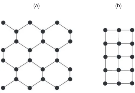
Yamaguchiet al.observed that the interface between NiSi and a Si(110) substrate is not flat after annealing at 550C.20) NiSi grows in the h110i direction on the Si(110) substrate and this phenomenon is named NiSi encroachment. They concluded that the encroachment can increase the leakage current, diminishing the CMOS performance. Considering the TEM images in Figs. 7(a) and 7(c), we speculate that the Pd2Si encroachment also occurs in Pd/Si(110) systems after
annealing at 600C with and without the Ti intermediate layer. Figure 8 shows schematic illustrations of the crystal-line Si structure viewed from theh110iandh001idirections on Si(110) and Si(001) substrates. The spacing of the Si lattice along theh110idirection is larger than that along the h001idirection.21)These results indicate that Pd atoms easily 500 nm
500 nm
500 nm 500 nm
(a)
(d) (b)
(c)
Fig. 6. SEM images of (a) Pd/Si(110), (b) Pd/Si(001), (c) Pd/Ti/Si(110), and (d) Pd/Ti/Si(001) samples after RTA at 600C for 30 s.
50 nm 120°
Pd2Si 100 facet (b)
(d) (a)
(c)
50 nm
50 nm 50 nm
diffuse in theh110i direction, and that the Pd2Si
encroach-ment in the h110i direction preferentially occurs compared with that in theh001idirection. As a consequence, although the diffusion of Pd atoms is suppressed with the Ti intermediate layer, some Pd atoms through the Ti layer immediately react with Si atoms to form Pd silicide. Therefore, the number of Pd atoms that react with Si is much larger on a Si(110) surface than on a Si(001) surface under the same annealing conditions. It is considered that silicidation on a Si(110) substrate is faster than that on a Si(001) substrate, as confirmed in Fig. 5. This causes the rough Pd2Si/Si(110) interface and layer thickness variation.
4. Conclusions
We investigated the growth and thermal stability of Pd silicide thin layers on Si(110) and Si(001) substrates with and without a Ti intermediate layer. Polycrystalline Pd2Si is
formed in Pd/Si systems at temperatures of 300–600C. On the other hand, an epitaxial or highly oriented Pd2Si layer is
formed in Pd/Ti/Si systems at annealing temperatures of 300–600C. The agglomeration of Pd
2Si in Pd/Ti/Si(001)
could be suppressed by the epitaxial growth of Pd2Si at
600C. It seems that the Ti intermediate layer does not effectively retard the diffusion of Pd atoms in Pd/Ti/Si(110) systems.
1) http://www.itrs.net/Links/2009ITRS/Home2009.htm
2) H. Mendez, D. M. Fried, S. B. Samavedam, T. Hoffmann, and B. Y. Nguyen: Solid State Technol.52(2009) 10.
3) L. Chang, Y. K. Choi, D. Ha, P. Ranade, S. Xiong, J. Bokor, C. M. Hu, and T. J. King:Proc. IEEE91(2003) 1860.
4) T. J. King: Electrochem. Soc. Interface14[1] (2005) 38.
5) K. Okuyama, A. Sugimura, and H. Sunami:Jpn. J. Appl. Phys.47(2008) 2407.
6) T. Sato, Y. Takeishi, and H. Hara:Jpn. J. Appl. Phys.8(1969) 588. 7) T. Sato, Y. Takeishi, H. Hara, and Y. Okamoto:Phys. Rev. B4(1971)
1950.
8) S. Kritzinger and K. N. Tu:J. Appl. Phys.52(1981) 305. 9) K. N. Tu:Appl. Phys. Lett.27(1975) 221.
10) M. Ostling and C. Zaring: inProperties of Metal Silicides, ed. K. Maex and M. V. Rosuum (Inspec, London, 1995) Chap. 1, p. 15.
11) R. Suryana, S. Akimoto, O. Nakatsuka, and S. Zaima: Ext. Abstr. Advanced Metallization 2008 Conf. 18th Asian Session, 2008, p. 88. 12) R. Suryana, O. Nakatsuka, and S. Zaima:Jpn. J. Appl. Phys.49(2010)
05FA09.
13) D. M. Hoffman, J. T. McGinn, F. J. Tams, III, and J. H. Thomas, III:
J. Vac. Sci. Technol. A5(1987) 1941.
14) S. Zaima, J. Kojima, M. Hayashi, H. Ikeda, H. Iwano, and Y. Yasuda:Jpn. J. Appl. Phys.34(1995) 741.
15) J. I. Langford and A. J. C. Wilson:J. Appl. Crystallogr.11(1978) 102. 16) B. D. Cullity and S. R. Stock:Elements of X-ray Diffraction(Prentice Hall,
Upper Saddle River, NJ, 2001) p. 167.
17) M. A. Nicolet and S. S. Lau: inVLSI Electronics Microstructure Science, ed. N. G. Einspruch and G. B. Larrabee (Academic Press, New York, 1983) Vol. 6, Chap. 6, p. 3329.
18) P. Gas and F. M. d’Heurle: inProperties of Metal Silicides, ed. K. Maex and M. V. Rossum (Inspec, London, 1995) Chap. 7, p. 279.
19) G. A. Hutchins and A. Shepela:Thin Solid Films18(1973) 343. 20) T. Yamaguchi, K. Kashihara, S. Kudo, T. Okudaira, T. Tsutsumi, K.
Maekawa, K. Asai, and M. Kojima:Jpn. J. Appl. Phys.48(2009) 066513. 21) L. E. Katz: inVLSI Technology, ed. S. M. Sze (McGraw-Hill, New York,
1988) Chap. 3, p. 110.
(b) (a)