Proceedings ofIEEE20086th National ConferenceonTelecommunication Technologies and IEEE20082nd Malaysia ConferenceonPhotonics,26-27 August 2008,Putrajaya, Malaysia
5-6 GHz Front End Low
Noise Amplifier
M.HChe
Halim',
M. Z.A.Abd
Aziz1' A. Rani Othman1, S.A Sahingan1, M.F Selamat1 and A.AAbd
Azizl
Faculty of Electronic & Computer Engineering Universiti TeknikalMalaysia Melaka (UTeM)
LockedBag 1200,HangTuahJaya,75450 Ayer Keroh, Melaka,Malaysia
hafizzan @gmail.com,[email protected],rani @utem.edu.my,[email protected],cyconx1 @gmail
.com,[email protected]
Abstract -This paper presents 5-6 GHz front end Low Noise Amplifier applicationfor IEEE standard 802.11 system for WLAN application. This amplifier uses FHX76LP Low noise SuperHEMT devicedesignedfor DBSapplicationfromEudynaDevice USA Inc. This paper is present design and simulation of single stage LNA circuits. Asinglestage LNA hassuccessfully designedwith 26.92 dB forwardgainand1.32 dB noisefigure,which stablealongtheUNII frequencyband.
Keyword:Wireless LAN; Low NoiseAmplifier;Gain; Noise Figure;MatchingCircuit.
I. INTRODUCTION
The IEEE 802.11 standard is used as references. The Low Noise Amplifier (LNA) system should meet this standard requirement and should operate properly for WLAN Bridge system [1]. The main requirements of the LNA are the lowest possible noise figure (NF) with a reasonable gain. The general topology of the LNA consists of threestages: theinput matching network (IMN), the amplifier itself and the output matching network (OMN)
[2],[3],[4].
The 5.8 GHz wireless LAN market grows rapidly and offers various benefits to the user 5.8 GHz LAN technology supports multimedia services, real time voice and video transfer and other bandwidth intensive applications[5].
This paper presents two different designs of aLNA at 5.8GHz. The circuit design starts from FHX76LP Low noise SuperHEMT device designed for DBS application from Eudyna Device USAInc amplifier using the microstrip technology. Itis the LNA that mainly determines the noise figure of the system. Low power dissipation and small integrated area are also some important factors that must be considered in the design of the devices for wireless applications [6]. Based on S-parameters of the transistor and certainperformancerequirements, a systematic procedure is developed for the design of LNA. In LNA design, the most important factors are low noise, moderate gain,
matching and stability [7]. Besides those factors, power
consumption and layout design size also need to be considered indesigned works.
The characteristic of this commercialize Low NoiseAmplifier areshowsinTable 1below
-Table 1: FHX76LP Characteristic
Component Parameter Value
Frequency Range 5000-6000 MHz
FHX76LP Associated Gain 12dB
NoiseFigure 0.4 dB
InputIP3 8dBm
OutputP1dB 9dBm
II. LNA Circuit Design A SinglestageLNA
A single stage microwave transistor amplifier can be modeled by the circuit in Figure 1 where a matching network is used both sides of the transistortotransform the input and output impedance ZA to the source and load impedance Zs and ZL. Themostusefulgain definition for amplifier design is the transducer power gain, which accountsbothsourceand load mismatch[8].
Figure1:Single StageLNA circuit
[image:1.613.325.576.542.678.2]Various type of matching technique can be applied to implement the matchingnetwork. The lump element matching is selected for this research work. The purpose of the calculation process is to predict the result for LNA design. MATLAB is usedtosimplify the calculationprocess. The calculation process begins with S-parameter selection for frequency 5 GHz to 6 GHz. In this paper, S-parameter is selected at bias point Vds= 2V and Ids= 10 mA from data sheet.
B Stability Consideration
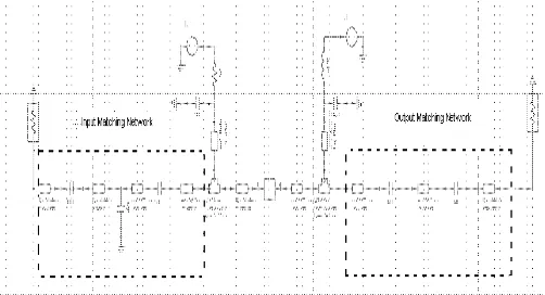
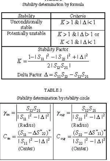
[image:2.613.327.566.170.458.2]One of the most important factors in high frequency amplifier design istodetermine stability of the given bias point. Equations in Table 2 and Table 3 are used to determine the stability and stability circle of the amplifier.
TABLE 2
Stability determination by formula
(2)
r1
OUT =1'*
LS
224S12S211rs
+12S21F5
1-1115s
By combining the two formulas above, reflection coefficient of input/output matching circuits can be calculatedby:
B1-
B12
-_41
C1
22C1
FLM
B2
-
B22 -41 C212
2C2
(3)
(4)
Where
Stability Criteria
Unconditionally K > 1 & A 1< 1 stable
Potentially unstable K > 1 & A> 1 or
K
<1& A
l<1
StabilityFactor
K 1-I
SI
12 -I 22 12 +1A 12 21S12S2211
Delta Factor A =
Si1
s22 -SI2
21TABLE 3
Stability determination by stability circle
S12S21
S12S21
Yin
-122
rout12-1IS
-l
1IA
12 S22 -1A12
(Radius) (Radius)
C _(Sil
-
AS*22
)
C
(S
22
-
AS11i)*
I1s51
-IA 22 -IA(Center) (Center)
Theinput and the outputcircuits should be matchedto deliver maximum power to the load. After stability of active device is determined, input and outputmatching circuits should be designed so that reflection coefficient of each port can be correlated withconjugate complex numberasgiven below:
B1 =1+
ISll
I'
-S22
12 - A12
(5)
B2
=1+1
2212
-_12
-A
2(6)
1C
= 11 -V22
(7)
C2
=E22
-VS11
(8)
v
=1
'11 22 -1232
1(9)
The formulas above givesourceand load reflection coefficientstoobtain maximumpowergain.
C NoiseFigure andConstant NoiseCircle
Signals and noises applied to the input port of amplifier are amplified by the gain of the amplifier and noise of amplifier itself is added to the output. Therefore, SNR (Signal to Noise Ratio) of the output port is smaller than that of theinputport.The ratio of SNR ofinputport to that ofoutput portis referredtoas noisefigure and is larger orless than 1.Typically, noisefigure of 2-port transistor has a minimum value at the specified admittance given by formula:
GN ls opt
F
=F.
+ RN It-
12
GS
(10)r - 8_ 12 21 L
FIN
=FS
=SII+
SIF
22 L
(1)
[image:2.613.68.291.265.589.2]D Designfor minimum Noise Figure
Low noise amplifier is important for receiver because noise figure of the amplifier of receiver affects noise figure of the whole system. To get minimum noise figure using 2-port transistor, source and load reflection coefficient should match with
Fopt
and load reflection coefficient should match withFout
with a complex conjugate number[9],[10]
as formula below:Fs
-F(11)
O74141
H5OGHz- 20GHz NWAI
KCS(cktCircui1)
H.OGHz
NVAM 580GHz
[image:3.612.45.301.177.299.2]INA!
Figure 3: LNAstabilitycircle
FL =OUt S22
+S12S21 )
1-S11rs)
(12)III. RESULT AND DISCUSSION
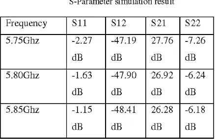
Fortheproposed single stage LNA shown in Figure 1, the simulation result is shown in Figure 2 to Figure 5. The design LNArequiredtwo 2V supply voltage andconsumes4.5mW. In thebeginning of the simulationprocess,the transistor is modeled in schematic using data sheet provided by manufacturer. The simulation result might not be accurate because the library has no data and modeled of the transistor FHX76LP Low noise SuperHEMT in Ansoft Designer. However. Duroid 5880 is being used as the microstrip substrate and the characteristic of this substrate. The comparison S-parameter simulated result as showninTable 3.
Ansoft Corporation XYPlot 2 Circuiti
08:ftS~
2000-.0o00 , ! I
5.0P 5..D 5.40 5..0 5.i
[image:3.612.61.301.453.656.2]F[GHz]
Figure 4: LNAsimulation resultat5.80GHz
Y1
dB(K)
NWA1
IXY5.81 221
"
Min AnsftCorpration
Circuii
1tg-uoX
1.4-z
C3
1A40
'540 R '''6'
F[GHz]
Figure2: LNAstability Figure5: LNA noisefigure
138
Y1
dB(Sl1J
NWAl
XY:5.80 -1 5
____1_
dB(S21)
NVA1
XY: 5801 269
Y1 dB(S22) NVVAl XY:5.80H656
Y1
NF NWA1
XY885M136
Yi V
dB(S12) NVWA1
XY580-4T87
07:54:26 Y1
dBi'NF)
NA1
XY53032
5.40 6.0
F[GHz] 6.0
AnsoftCogrporaion
i
m
io
.3A
.
.m
[image:3.612.340.569.457.652.2]TABLE 3
S-Parameter simulation result
A 5.8GHz low noise single stage amplifiers based on
FHX76LP Low noise SuperHEMT transistor was designed and
the prototype was tested at room temperature. At 2V collector bias on 5.8 GHz ,this LNA has noise figure 1.32dB, with input
return loss of -1.63dB, insertion loss of -47.90dB and output returnloss of -6.24dB. Usually,aslongasthestability factor and
delta factor are known as unconditionally stable, the stability
circle is necessarytobeproved because the amplifier is stableat
allareawithin the smith chart [9].
IV. CONCLUSION
The research work has yield a newLow Noise Amplifier
(LNA) circuit' design for frequency of 5.75 GHz to 5.85 GHz and circuit simulation were done in Ansoft Designer. LNA has
successfully simulated with 26.92 dB gain and 1.32 dB noise figureatfrequency 5.8 GHz
REFERENCES
[1] Heng Jin and C.A.T. Salama, "A 1-V, 1.9- GHz CDMA, CMOSonSOI, low noiseamplifier," in SOI Conference, 2000 IEEE International.
[2] T. Lee, The Design of CMOS Radio-Frequency Integrated Circuits,
Cambridge University Press, 1998.
[3] B. Jung Jang,I.BokYom, S. Pal Lee (2001). "V-Band MMIC Low Noise
Amplifier Design Based on Distributed Active Device Model",
Proceedings of APMC2001, IEEE, 2001. 25-28.
[4] Sungkyung Park and Wonchan Kim, "Design of a 1.8 GHz low-noise
amplifier for RF front-end in a 0.8," Consumer Electronics, IEEE
Transactionson,vol.47,no.0098, 2001.
[5] A. Parssinen, S. Lindfors, J. Ryynanen, S.I.Long, and K. Halonen, "1.8 GHz
CMOS LNA with on-chip DCcoupling for a subsampling direct," in
Circuits and Systems, 1998. ISCAS '98. Proceedings ofthe 1998 IEEE
InternationalSymposiumon,1998, vol. 2,pp.73-76.
[6]D.M.Pozar(2000). "Microwave and RF WirelessSystem",United States of
America: JohnWiley and Sons Inc. 77-97, 205-207.
[7] G. Gonzalez (1997). " Microwave Transistor Amplifier: Analysis and
Design", 2ndEdition, Upper Saddle River, NJ: Prentice- Hall Inc. 217,
294-303.
[8] D. M. Pozar(1998)."MicrowaveEngineering",2ndEdition,United States of America: JohnWileyand Sons Inc.258-266,600-605.
[9] T.K.K. Tsang and M.N. El-Gamal, "Gain and frequencycontrollable sub-I V 5.8 GHz CMOSLNA,"inCircuits andSystems, 2002. ISCAS 2002. IEEE
InternationalSymposiumon,2002, vol. 4,pp.IV-795-IV-798.
[10]E.H. Fooks and R.A. Zakarevicius (1990). "Microwave Engineering Using Microstrip Strips", Australia: Prentice Hall. 46,131-133.
139
Frequency S11 S12 S21 S22
5.75Ghz -2.27 -47.19 27.76 -7.26
dB dB dB dB
5.80Ghz -1.63 -47.90 26.92 -6.24
dB dB dB dB
5.85Ghz -1.15 -48.41 26.28 -6.18