i
STATISTICAL ANALYSIS AND OPTIMIZATION OF 5.8 GHz RF AMPLIFIER
KASRIDONA BIN RULLY
This report is submitted in partial fulfilment of the requirements for the award of Bachelor of Electronic Engineering (Telecommunication Electronics) With Honours
Faculty of Electronic and Computer Engineering Universiti Teknikal Malaysia Melaka
ii
UNIVERSTI TEKNIKAL MALAYSIA MELAKA
FAKULTI KEJURUTERAAN ELEKTRONIK DAN KEJURUTERAAN KOMPUTER
BORANG PENGESAHAN STATUS LAPORAN PROJEK SARJANA MUDA II
Tajuk Projek : STATISTICAL ANALYSIS AND OPTIMIZATION OF 5.8GHz RF AMPLIFIER
Sesi
Pengajian : 2008/2009
Saya ………...KASRIDONA BIN RULLY……….. (HURUF BESAR)
mengaku membenarkan Laporan Projek Sarjana Muda ini disimpan di Perpustakaan dengan syarat-syarat kegunaan seperti berikut:
1. Laporan adalah hakmilik Universiti Teknikal Malaysia Melaka.
2. Perpustakaan dibenarkan membuat salinan untuk tujuan pengajian sahaja.
3. Perpustakaan dibenarkan membuat salinan laporan ini sebagai bahan pertukaran antara institusi
pengajian tinggi.
4. Sila tandakan ( √ ) :
SULIT*
(Mengandungi maklumat yang berdarjah keselamatan atau kepentingan Malaysia seperti yang termaktub di dalam AKTA RAHSIA RASMI 1972)
TERHAD* (Mengandungi maklumat terhad yang telah ditentukan oleh
organisasi/badan di mana penyelidikan dijalankan)
TIDAK TERHAD
Disahkan oleh:
__________________________ ___________________________________
(TANDATANGAN PENULIS) (COP DAN TANDATANGAN PENYELIA)
Alamat Tetap: Lot 217A Lorong 6, Kg. Pasir Putih Sabah Baru,Jalan Sin San, 91000 Tawau
Sabah.
iii
“I hereby declare that this report is the result of my own work except for quotes as cited in the references”
Signature :……….
iv
“I hereby declare that I have read this report and in my opinion this report is sufficient in terms of the scope and quality for the award of Bachelor of Electronic Engineering
(Telecommunication Electronics) With Honours.”
Signature :……….
v
vi
ACKNOWLEDGEMENT
vii
ABSTRACT
viii
ABSTRAK
ix
CONTENTS
CHAPTER TITLE PAGE
PROJECT TITLE i
DECLARATION iii
DEDICATION v
ACKNOWLEDGEMENT vi
ABSTRACT vii
ABSTRAK viii
CONTENTS ix
LIST OF TABLES xiii
LIST OF FIGURES xiv
LIST OF ABBREVIATIONS xvi
LIST OF APPENDICES xviii
I INTRODUCTION
1.1 Project Background 1
1.2 Project Objectives 2
1.3 Problem Statements 2
1.4 Scope of work 2
1.5 Project Methodology 3
x
II LITERATURE REVIEW
2.1 Introduction 5
2.2 RF Amplifier 5
7
2.2.1 Review of RF amplifiers 7
2.2.2 Design of microwave transistor amplifier 11 using s-parameter
2.2.3 Review of transmission lines 11 2.2.4 Review of scattering matrix 12
2.3 Stability 14
2.3.1 Stability analysis 16
2.4 Gains 16
2.5 Noise In Amplifiers 18
2.6 Voltage Standing Wave Ratio (VSWR) 20
2.7 Input And Output Matching 20
2.7.1 Impedance transformation and matching 22
2.8 Attenuator 24
III RESEARCH METHODOLOGY
3.1 Introduction 26
3.2 RF Amplifier Overview 27
3.3 Transistor Selection 27
3.4 Theoretical Analysis of RF Amplifier 28 3.4.1 Scattering parameter (S-parameter) 28
3.4.2 Stability analysis 29
3.4.3 Overall gains 31
xi
3.4.5 Voltage standing wave ratio (VSWR) 33
3.4.6 Noise figure 33
3.5 Circuit Design 34
3.5.1 Stability analysis 34
3.5.2 Impedance matching 35
3.5.2.1 Input impedance matching 36 3.5.2.2 Output impedance matching 37
3.5.3 Transmission line 38
3.6 Simulate And Optimize The Designed RF 41 Amplifier
3.7 Compare of Result Based On Theoretical And 41 Simulation
IV RESULT, ANALYSIS AND DISCUSSION
4.1 Introduction
42
4.2 Theoretical Analysis Results 42
4.2.1 Scattering parameter (S-parameter) 43 4.2.2 Stability analysis results 43
4.2.3 Overall gains 44
4.2.4 Input and output impedance 45 4.2.5 Voltage standing wave ratio (VSWR) 46
4.2.6 Noise figure 46
4.3 Circuit Design 46
4.3.1 Impedance matching 47
4.3.1.1 Input impedance matching 47 4.3.1.2 Output impedance matching 48
4.3.2 Designed circuit 49
xii
4.4.1 Stability 50
4.4.2 S-parameter 50
4.4.3 Voltage standing wave ratio (VSWR) 53
4.4.4 Noise figure 54
4.5 Optimization 55
4.6 Result Comparison 59
V CONCLUSION
5.1 Introduction
60
5.2 Summary 60
5.3 Conclusion 61
VI REFERENCES 63
xiii
LIST OF TABLES
NO TITLE PAGE
2.1 Summary of RF amplifiers 10
2.2 π type and T type attenuator formula 25
3.1 S-parameter for FET EPA018A-70 at 5.8 GHz 29
3.2 Stability circle formula 30
4.1 S-parameter for FET EPA018A-70 at 5.8 GHz 43
4.2 Circuit elements value 49
4.3 Optimized circuit elements value 59
xiv
LIST OF FIGURES
NO TITLE PAGE
2.1 RF amplifier in communication system blocks 6
2.2 Circuit layout 7
2.3 Stability circle 15
2.4 Typical amplifier systems 17
2.5 Matching network to load 21
2.6 Single lumped element 22
2.7 Dual lumped elements 22
2.8 Triple lumped elements 23
2.9 Distributed elements 23
2.10 Hybrid 23
2.11 π type and T type attenuator 24
3.1 Typical amplifier systems 27
3.2 Input stability circles 30
3.3 Output stability circles 31
3.4 Input and output stability circles 35
3.5 Input impedance matching 36
3.6 Output impedance matching 37
3.7 Sample calculations for transmission line using MathCAD 39
xv
4.2 Output impedance matching 48
4.3 Designed RF amplifier circuit 49
4.4 Simulation stability 50
4.5 S11 plot 51
4.6 S22 plot 51
4.7 S21 and maximum gain plot 52
4.8 VSWRin plot 53
4.9 VSWRout plot 53
4.10 Simulation NFmin 54
4.11 Noise and available gain circles 54
4.12 Optimized stability 55
4.13 Optimized gain 56
4.14 Optimized VSWRin 57
4.15 Optimized VSWRout 57
4.16 Optimized noise figure 58
xvi
LIST OF ABBREVIATIONS
ADS - Advanced Design System
AlN - Aluminium Nitrate
AlGaN/GaN - Aluminum Gallium Nitride / Gallium Nitride BJT - Bipolar Junction Transistor
BPF - Band Pass Filter
CMOS - Complementary Metal Oxide Semiconductor
dB - Decibel
DC - Direct Current
FET - Field Effect Transistor
FSK - Frequency Shift Keying
GaAs - Gallium Arsenide
HBT - Heterojunction Bipolar Transistor HEMT - High Electron Mobility Transistor
IEEE - Institute of Electrical and Electronic Engineering InGaAs - Indium Gallium Arsenide
LNA - Low Noise Amplifier
MESFET - MEtal Semiconductor Field Effect Transistor MMIC - Monolithic Microwave Integrated Circuits
PA - Power Amplifier
PAE - Power Added Efficiency
RF - Radio Frequency
xvii
TL - Transmission Line
TWPA - Travelling-Wave Power Amplifier
UWB - Ultra Wide Band
xviii
LIST OF APPENDICES
APPENDIX TITLE PAGE
A Exelics EPA018A-70 data sheet 65
B Calculation of theoretical measurements 67
1
CHAPTER I
INTRODUCTION
1.1Project background
Radio Frequency (RF) means any frequency within the electromagnetic spectrum associated with radio wave propagation. When an RF current is supplied to an antenna, an electromagnetic field is created that then is able to propagate through space [1].
2
1.2Project objectives
The main objective of this project is to study the background of a RF amplifier and proposed a suitable RF amplifier unit and optimizes the circuit with overall gain of 20dB with noise figure less than 3dB.
1.3Problem statements
As we know, the main function of RF amplifier is to amplify the received signal to a certain level of gain. RF amplifier is needed in the communication system because of its function which is to amplify the received signal. The received signal in the receiver antenna is lower than the transmitted signal due to the attenuation and noise in the channel. The RF amplifier used to amplify the information signal in order to have a clearer signal.
The major problem in this project is to design the suitable RF amplifier for the specified requirements. The method used in designing the RF amplifier and matching network also are the crucial part in designing the RF amplifier.
1.4Scope of work
The scopes of work for this project are limited to the following aspects:
1. Types of amplifier.
3
2. Types of transistor.
Types of transistor used in most RF amplifier viewed and its characteristic studied.
3. Matching technique.
Types of matching technique studied the advantages and disadvantages for every matching technique observed.
4. Specification for circuit and testing.
The specification for circuit and testing are set based on previous achievement of RF amplifier design.
1.5Project methodology
Phase 1:
Transistor selection.
Phase 2:
Theoretical analysis of RF amplifier.
Phase 3:
Circuit design and analysis.
Phase 4:
Simulate and optimize the designed RF amplifier
Phase 5:
4
1.6Report structure
This report divided into 5 chapters. The first chapter gives a brief explanation about RF amplifier and its function in communication systems. It also gives brief explanations about the overall process of project.
The second chapter is about the literature review of the project. Background knowledge of RF amplifier studied in order to understand the basic in RF amplifier design. Other parameter used in the design such as stability, gains, and matching technique are also studied.
The third chapter is about research methodology which explained about method used and process involved in the project.
The fourth chapter is about the result, analysis and discussion. All the data and results that obtained at the end of this project will be documented in this chapter.
5
CHAPTER II
LITERATURE REVIEW
2.1 Introduction
This chapter reviews about the information obtained from findings and any useful sources. Information from the literature is very important as the background of RF amplifier design. Basic principles used in the analysis and design of RF amplifier developed in this chapter.
2.2 RF Amplifier
The power amplifier is the most important and expensive device in the RF block of Wireless LAN system [2]. The design of RF amplifiers involves less emphasis on noise parameters and more emphasis on linearity and inter-modulation, as well as efficiency and thermal considerations. To design a RF amplifier, one must use large-signal S-parameters and be aware of nonlinear effects.
6
optimizing the output matching network. There are, however, special problems associated with the very low input impedance that can be found in FET power devices, which require special treatment in the input matching network if wideband operation is to be achieved [3].
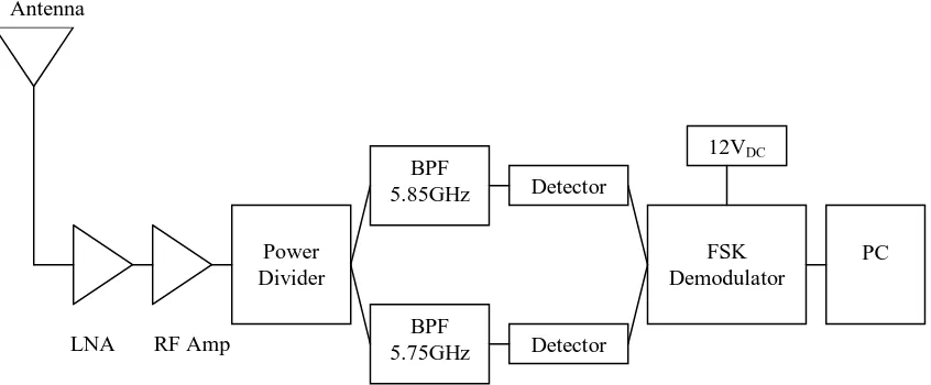
[image:24.612.120.543.375.550.2]A key issue for multi-stage amplifiers is the ability to cascade individually designed stages without a requirement for retuning or redesign to account for the characteristic of the driving or following stages. In many cases, the use of balanced amplifiers permits the benefit of 3 dB coupler inter-stages, which direct reflected power to the isolated port rather than the driving stage. As we will see in later, there are special problems of nonlinear oscillations arising from interaction between signal harmonics and modes of the output matching structure [3]. Figure 2.1 below shows the block diagram of an amplifier circuit:
Figure 2.1 RF amplifier in communication system blocks.
RF Amp
BPF
5.85GHz Detector