Yudo ketsugo intafesu no sekkei jidoka to saitekika
Bebas
144
0
0
Teks penuh
(2)
(3) Acknowledgements I would like to thank my adviser, Prof. Tadahiro Kuroda, for his greatest support and guidance while I study toward doctoral degree. I also would like to thank Prof. Masato Motomura for giving me his priceless guidances in developing novel TCI based 3-D FPGA architecture exploration framework. The experience of studying in Keio University is invaluable to me. I feel lucky to join Kuroda Lab to learn cutting-edge techniques and grow stronger in various aspects. I would like to thank my wife, Yen-Ling, to keep me motivated and encourage me while I am depressed. Especially, thanks you for great help in taking good care our lovely daughter, Yu-Hsuan. I would also like to thank my parents’ continuous support and encouragement. Without you, I am unable to realize my dream in studying abroad. I would like to thank Kuroda laboratory members for their support in working environment, life, knowledge sharing, and creative ideas in these years. Yasuhiro Take, Tsutomu Takeya, Hekilin Chang, Chika Kijima, Ritsuko Mukai, Tsunaaki Shidei, Noriyuki Miura, Mitsuko Saito, Atsutake Kosuge, Junaidi Abdul Raziz, So Hasegawa, Junichiro Kadomoto, Katsuki Ohata, and many others. You really. iii.
(4) make my life easy and joyful. Thanks you. I would like to thank my thesis reviewers, Prof. Amano, Prof. Ishikuro, and Prof. Nakano, for giving me priceless suggestions to improve the thesis in organization and content and helping me to find out the blind spots that I did not consider before. Without your enlightenment, I am unable to break out the window to think more extensively. Finally, I would like thank Interchange Association, Japan, and JASSO for providing me the scholarship. Without your support, I am unable to continue on my study and life in Japan. Hopefully, I can have the ability to contribute back to Japan in the future.. Keio University, Yokohama, Japan September 2015 Hsu Li-Chung. iv.
(5) Abstract As manufacturing cost in keeping up with the Moores Law grows exponentially, the idea of three-dimensional (3-D) integrated circuit (IC) technologies become promising solutions in facing the ultimate physical challenges. In recent years, the ThruChip interface (TCI) becomes one of emerging 3-D stacking technologies. TCI is a wireless interface for stacking chips vertically. Due to its wireless nature, TCI can integrate IC products with low fabrication cost in comparing to wiring solution while offering good communication reliability and high data bandwidth. Although TCI has been researched in diverse applications for years, the TCI design automation and influences of physical structures, such as power mesh and dummy metal fill, have not been explored. Without this information, designers may design TCI too conservatively and CAD engineers are unable realize design automation. As a result, in order to enrich TCI design methodologies, this thesis focuses on discussing TCI extensive design automation and optimization topics in physical design guidelines, inductive coupling coil, and 3-D FPGA system. Chapter 1 introduces the background of challenges in modern semiconductor. v.
(6) industry, the potential solutions in wiring/wireless 3-D IC integration technology, the basic concept of TCI, and the scope of this thesis. Chapter 2 presents TCI physical design guideline experiments in exploring the dependence between power consumption and D/Z ratio, power mesh impact, and dummy metal impact. The experiment results show that keeping the TCI coil diameter (D) and communication distance (Z) ratio to three is the optimal ratio and enlarging D/Z to six can further reduce total power by 20%. The eddy current on power mesh can cause TCI to fail. Creating a minimum space chop on power mesh can effectively recover TCI communication from eddy current impact with only additional 0.6% voltage drop. Dummy metal fill structure has no impact on TCI. Chapter 3 introduces an analytical TCI inductive coupling coil design optimization methodology. The optimization results show that the proposed flow can improve mutual inductance value by 17% on average in comparing to baseline cases in chapter 2 and save the design time from days to minutes. Chapter 4 presents the novel TCI based 3-D field programmable gate array (FPGA) architecture exploration framework. This chapter gives an overview of placement, routing, timing optimization, and noise avoidance design flow in TCI based 3-D FPGA system and raises issues that the architecture may encounter while adopting TCI. The experimental results show the proposed 3-D FPGA architecture can reduce delay by 25% on average over 2-D FPGA. Although the performance of TCI based 3-D FPGA architecture is 8% worse than through-. vi.
(7) silicon-via (TSV) based 3-D FPGA on average, TCI based architecture can reduce active area consumed by vertical communication channels by 42% on average and thus lead to better area and delay product. Chapter 5 summarizes this thesis and revisits the objectives of this study. An overview of future work is also given.. vii.
(8) Contents. Acknowledgements. iii. Abstract. v. Contents. viii. List of Figures. xii. List of Tables. xvii. 1 Introduction. 1. 1.1 Background . . . . . . . . . . . . . . . . . . . . . . . . . . . . . . .. 2. 1.1.1. Active Device Scaling Trend . . . . . . . . . . . . . . . . . .. 3. 1.1.2. Scaling Challenges . . . . . . . . . . . . . . . . . . . . . . .. 4. 1.1.3. Future Opportunities . . . . . . . . . . . . . . . . . . . . . .. 5. 1.2 3-D IC Technologies Overview . . . . . . . . . . . . . . . . . . . . .. 8. 1.2.1. Wired 3-D Interface . . . . . . . . . . . . . . . . . . . . . . .. 9. 1.2.2. Wireless 3-D Interface . . . . . . . . . . . . . . . . . . . . .. 11. 1.3 ThruChip Interface Technology Overview . . . . . . . . . . . . . .. 12. viii.
(9) CONTENTS 1.4 TCI Design Automation Issues . . . . . . . . . . . . . . . . . . . . .. 14. 1.4.1. Physical Design Considerations . . . . . . . . . . . . . . . .. 15. 1.4.2. Inductive Coupling Channel Optimization . . . . . . . . .. 15. 1.4.3. Timing Optimization and Noise Avoidance in 3-D FPGA System . . . . . . . . . . . . . . . . . . . . . . . . . . . . . .. 16. 1.5 Thesis Organization . . . . . . . . . . . . . . . . . . . . . . . . . . .. 17. References for Chapter 1. 22. 2 ThruChip Physical Design Guideline Exploration. 31. 2.1 TCI Design Guideline Exploration . . . . . . . . . . . . . . . . . . .. 32. 2.2 Measurement Results and Design Analysis . . . . . . . . . . . . . .. 35. 2.2.1. The Baseline Scenarios . . . . . . . . . . . . . . . . . . . . .. 35. 2.2.2. The Power Mesh Impact . . . . . . . . . . . . . . . . . . . .. 39. 2.2.3. The Dummy Metal Fill Impact . . . . . . . . . . . . . . . . .. 44. 2.3 Conclusion . . . . . . . . . . . . . . . . . . . . . . . . . . . . . . . .. 48. References for Chapter 2. 50. 3 Analytical Inductive Coupling Channel Optimization. 51. 3.1 The Essential Functions in Designing TCI Inductive Coupling Channel . . . . . . . . . . . . . . . . . . . . . . . . . . . . . . . . . . . . .. 53. 3.2 Inductive Coupling Channel Optimization . . . . . . . . . . . . . .. 55. 3.2.1. Inductor Layout Variables . . . . . . . . . . . . . . . . . . .. 56. 3.2.2. Inductor Electrical Model . . . . . . . . . . . . . . . . . . .. 59. ix.
(10) CONTENTS 3.2.3. Inductive Coil Channel Optimization Flow . . . . . . . . .. 61. 3.3 Experiment Results . . . . . . . . . . . . . . . . . . . . . . . . . . .. 66. 3.3.1. Transmitting Power vs. D/Z . . . . . . . . . . . . . . . . . .. 67. 3.3.2. Coil Area vs. D/Z . . . . . . . . . . . . . . . . . . . . . . . .. 68. 3.3.3. Transmitting Power vs. Coil Area . . . . . . . . . . . . . . .. 70. 3.3.4. Optimization Result Comparisons . . . . . . . . . . . . . .. 72. 3.3.5. Conclusion . . . . . . . . . . . . . . . . . . . . . . . . . . . .. 74. References for Chapter 3. 79. 4 A Novel TCI Based 3-D FPGA Architecture Exploration Framework. 82. 4.1 Conventional 2-D FPGA Architecture Exploration Tool . . . . . . .. 83. 4.2 3-D FPGA Placement and Routing Tool . . . . . . . . . . . . . . . .. 84. 4.3 Reconfigurable TCI Transceiver . . . . . . . . . . . . . . . . . . . .. 86. 4.3.1. The Proposed Reconfigurable TCI Transceiver Architecture. 87. 4.3.2. Coils Overlapping . . . . . . . . . . . . . . . . . . . . . . . .. 90. 4.4 TCI Based 3-D FPGA Exploration Tool Framework . . . . . . . . .. 94. 4.4.1. Reconfigurable TCI Transceiver Routing Structure . . . . .. 96. 4.4.2. Timing Slot Rescheduling . . . . . . . . . . . . . . . . . . .. 97. 4.5 Experiment Results . . . . . . . . . . . . . . . . . . . . . . . . . . . 103 4.5.1. Experiment Setup . . . . . . . . . . . . . . . . . . . . . . . . 103. 4.5.2. Comparisons among FPGA Architectures . . . . . . . . . . 107. References for Chapter 4. 112. x.
(11) CONTENTS 5 Conclusion. 115. 5.1 Scope of Future Works . . . . . . . . . . . . . . . . . . . . . . . . . 117 References for Chapter 5. 119. Appendix. 121. A IR-Drop Evaluation in OpenCore and TCI Circuit Integration. xi. 121.
(12) List of Figures 1.1 Global smartphone, tablet, and PC shipment trends. . . . . . . . .. 3. 1.2 Gate cost scaling trend over technology nodes [25].. . . . . . . . .. 5. 1.3 BEOL delay/area/cost scaling trend. . . . . . . . . . . . . . . . . .. 6. 1.4 SRAM bit cell area scaling trend. . . . . . . . . . . . . . . . . . . .. 7. 1.5 3-D inter-chip interconnection technologies (a) Micro-Bump (b) Through-Silicon-Via (TSV) (c) Capacitive-Coupling Interface (d) Inductive-Coupling Interface. . . . . . . . . . . . . . . . . . . . . .. 9. 1.6 Basic ThruChip Interface (TCI) architecture and its operation diagram [17].. . . . . . . . . . . . . . . . . . . . . . . . . . . . . . . . .. 14. 1.7 Overview of TCI based 3-D FPGA architecture [41]. . . . . . . . .. 18. 1.8 The thesis organization.. 19. . . . . . . . . . . . . . . . . . . . . . . . .. 2.1 Test chip microphotograph and chips stacking cross-section view (a) Baseline (b) Dummy metal scenario (c) Power mesh scenario. .. xii. 33.
(13) LIST OF FIGURES 2.2 (a) The top-bottom layout view of the power mesh scenario. The power mesh is on the RX Chip. (b) Illustration of induced eddy current on power mesh.. . . . . . . . . . . . . . . . . . . . . . . . .. 35. 2.3 (a) The top-bottom layout view of the dummy metal fill scenario. The dummy metal fill is deployed on both chips. (b) Illustration of induced eddy current on dummy metal fill. . . . . . . . . . . . . .. 36. 2.4 Bit Error Rate (BER) vs. Transmitting Power[mW]. . . . . . . . . .. 37. 2.5 Normalized Total Power vs. D/Z in both measurement and simulation results.. . . . . . . . . . . . . . . . . . . . . . . . . . . . . . .. 38. 2.6 Illustration of current density map in power mesh and power stripes only scenarios (a) The induced eddy current on the conductive loops forming on the power mesh will consume most of the magnetic pulse energy and thus cause RX coil fail to sense the magnetic signal (b) Most of the magnetic pulse can reach RX coil if there are power stripes only (no formation of conductive loops) between TX and RX coils.. . . . . . . . . . . . . . . . . . . . . . . . . . . . . . .. 40. 2.7 Recover coupling coefficient (K) by removing stacked power vias to guide eddy current away from TCI coil. (a) Normalized Coupling Coefficient (K) Vs. X/D (D120, D180, and D240) (b) Eddy current density map when X/D=0.25 (c) Eddy current density map when X/D=0.9. . . . . . . . . . . . . . . . . . . . . . . . . . . . . .. xiii. 42.
(14) LIST OF FIGURES 2.8 Recover coupling coefficient (K) by creating a minimum space gap on power mesh lines to guide eddy current away from TCI coil.. .. 43. 2.9 Dynamic IR-drop heat map in OpenCore design with D240 inductive coupling coils embedded (a) Baseline case (b) Pushing eddy current away by removing stacking power vias (X/D=0.9) (c) Pushing eddy current away by creating minimum space gap on power mesh lines (X/D=0.9).. . . . . . . . . . . . . . . . . . . . . . . . . .. 45. 2.10 Dynamic IR-Drop Ratio vs. X/D in D240 scenario. . . . . . . . . .. 46. 2.11 Dynamic IR-drop heat map in OpenCore design with (a) minimum space chop (X/D=0.9) in one D240 inductive coupling coil embedded (b) minimum space chop (X/D=0.9) in four D120 inductive coupling coils embedded. (c) is the IR-Drop histogram graph of these two scenarios. . . . . . . . . . . . . . . . . . . . . . . . . . . . 2.12 Normalized Transmitting Power vs. Dummy Metal Density.. 47. . . .. 48. 3.1 TCI signal operation diagram. . . . . . . . . . . . . . . . . . . . . .. 54. 3.2 The conventional TCI inductive coupling channel design flow. . .. 56. 3.3 (a) Square Inductor Layout and Geometry (b) Placement of TX and RX Square Coils.. . . . . . . . . . . . . . . . . . . . . . . . . . . . .. 58. 3.4 Inductor models (a) conventional Π model [6] (b) simplified model used in TCI [5]. . . . . . . . . . . . . . . . . . . . . . . . . . . . . .. 60. 3.5 The proposed analytical TCI inductive coupling inductor design flow.. . . . . . . . . . . . . . . . . . . . . . . . . . . . . . . . . . . .. xiv. 61.
(15) LIST OF FIGURES 3.6 Heat map of IP over nT X and nRX (a) DRX =120um (D/Z=2) (b) DRX =180um (D/Z=3) (c) DRX =240um (D/Z=4). 3.7 DRX. OUT. and DT X. IN. . . . . . . . . . .. 68. definitions. . . . . . . . . . . . . . . . . . . .. 69. 3.8 Heat map of coil area over nT X and nRX (a) DRX =120um (D/Z=2) (b) DRX =180um (D/Z=3) (c) DRX =240um (D/Z=4).. . . . . . . . .. 70. 3.9 (a) The five solutions which meet IT X design target 1.5mA in D/Z=3 and 4 cases (b) The projected solutions on coil area heat maps in D/Z=3 and 4 cases. . . . . . . . . . . . . . . . . . . . . . . . . . . .. 72. 3.10 The mutual inductance value comparison among previous works [8– 10] and the optimization results. The data is obtained by 3-D field solver simulation. . . . . . . . . . . . . . . . . . . . . . . . . . . . .. 75. 3.11 The spice simulation result in D120 (D/Z=2) case. Red and blue lines represent the original and optimization cases respectively. The optimization result shows 15.7% transmitting current (IT X ) reduction to achieve comparable VR value.. . . . . . . . . . . . . .. 76. 3.12 The required TX current comparison results between the previous work [8] and the optimization results in spice simulation. . . . . .. 77. 4.1 VTR CAD flow for FPGA architecture exploration . . . . . . . . . .. 85. 4.2 The proposed reconfigurable TCI transceiver (a) The relation to CLBs and SBs (b) The detailed illustration . . . . . . . . . . . . . .. 88. 4.3 Operation timing diagram of the proposed reconfigurable TCI transceivers 89. xv.
(16) LIST OF FIGURES 4.4 Multi-Layers transmission scenarios (a) Data latch relay (b) Direct link . . . . . . . . . . . . . . . . . . . . . . . . . . . . . . . . . . . .. 91. 4.5 (a) Non-overlapped TCI channels (b) Overlapped TCI channels with quadrature phase division multiplexing . . . . . . . . . . . . . . .. 93. 4.6 Flow diagram of TCI based 3-D FPGA exploration tool . . . . . . .. 95. 4.7 (a) Example of a FPGA routing structure (b) Illustration of routing graph construction . . . . . . . . . . . . . . . . . . . . . . . . . . .. 98. 4.8 Timing slot rescheduling algorithm . . . . . . . . . . . . . . . . . .. 99. 4.9 Illustration of one example timing path before and after applying timing slot rescheduling algorithm.. . . . . . . . . . . . . . . . . . 102. 4.10 Worst path delay vs. timing slot rescheduling iterations . . . . . . 103 4.11 Detail delay configuration in the evaluated FPGA architecture. . . 104 4.12 (a) TSV yield recovery architecture [12] (b) Recovery mechanism: TSV 2 fails and TSV 2 and TSV 3 are shifted one right position for vertical path recovery . . . . . . . . . . . . . . . . . . . . . . . . . . 105 A.1 The floorplan of TCI TX and RX blocks in OpenCore design. . . . 122 A.2 Dynamic IR-drop heat maps in OpenCore design with (a) only D240 TCI coil deployed (primitive case) and (b) both D240 TCI coil and transceiver circuits deployed. . . . . . . . . . . . . . . . . 123 A.3 IR-Drop histogram comparison in primitive and TCI circuit block deployed cases.. . . . . . . . . . . . . . . . . . . . . . . . . . . . . . 124. xvi.
(17) List of Tables 2.1 The detail configurations of TX and RX coil pairs. . . . . . . . . . .. 34. 3.1 The detail configurations of TX and RX coils from the baseline coils in [8–10] and the proposed optimization flow. . . . . . . . . . . . .. 73. 4.1 Definitions of Some Terms . . . . . . . . . . . . . . . . . . . . . . .. 97. 4.2 Area evaluation of reconfigurable TCI transceiver . . . . . . . . . . 107 4.3 MCNC benchmarks evaluation results in 2-D FPGA and TCI based 3-D FPGA architectures . . . . . . . . . . . . . . . . . . . . . . . . . 110 4.4 MCNC benchmarks evaluation results in TSV based 3-D FPGA and TCI based 3-D FPGA architectures . . . . . . . . . . . . . . . . . . 111. xvii.
(18) Chapter 1 Introduction. 1.
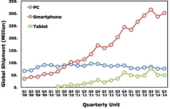
(19) 1.1. Background. 1.1 Background Since the first iPhone was introduced, its fantastic user interface experience started the first smartphone explosive growth in 2007. The strong demand in smart portable devices, such as tablets and smart wearable, with increasing performance and fascinating user experiences come after. The mobile smart devices and fantastic applications have been sprung up like mushrooms in recent years. It was reported that smartphone shipment and tablet surpassed PC shipment for the first time in Q4 of 2010 and in Q4 of 2013 respectively according to International Data Corporation (IDC) [24]. Mobile System-on-chip (SoC) has taken the place of personal computer (PC) market and become the leading driver in semiconductor industry. Figure 1.1 shows the global smart phone, tablet, and PC shipment trends from 2009 to 2014. In PC market, CPU is designed to perform at very high frequency and GPU is designed to highly parallel and squeezed into a given silicon area for better performance. The performance of CPU and GPU is both constrained by the cooling system. In contrast to PC market, cost and energy-efficiency in mobile SoC is always the leading indexes in portable consumer market. As a result, it can be seen that mainstream smartphone SoC manufacturers seek for lowest die cost by optimizing factors, such as mask cost, wafer process, package process, and yield [23], to strengthen their competition in the mobile market.. 2.
(20) 1.1. Background. Figure 1.1: Global smartphone, tablet, and PC shipment trends.. 1.1.1 Active Device Scaling Trend Conventionally, chip makers tend to reduce their chip cost and improve performance by geometrical scaling. This is also a rule-of-thumb lasting for fifty years in semiconductor industry. Although technology scaling has hit the power limitations caused by unscalable sub-threshold slope and increasing leakage power, several innovations, such as high-K/metal gate [19] and FinFET [20], in the last decade have kept extending IC scaling. FinFET can not only enable fully depleted (FD) channel to offer better short channel effects (SCE) control but also push the sub-threshold swing close to the room temperature thermal limit, 62 mV/dec [21]. Based on the outstanding device characteristics of FinFET, semi-. 3.
(21) 1.1. Background conductor industry can continue moving beyond 20nm to offer better performance and more power reduction (40% higher speed and 60% power saving in comparison with 20nm [22]). Although gate delay, area, and power are keeping improved by scaling device beyond 28nm, the gate cost scaling trend has started to grow in worse direction. According to International Business Strategies (IBS) white paper [25] and fabless IC design houses reports in recent years [30], the gate cost reduction trend has already slowed down and start to bound after 28nm. Figure 1.2 shows the cost scaling trend over technology nodes [25]. As a result, mobile SoC manufacture companies have started to reconsider scaling pro and con while adopting advanced technology node after going beyond 28nm.. 1.1.2 Scaling Challenges Although active devices scaling can possibly lead to more competitive IC product, it is reported that the delay/area/cost gap between the back-end-of-line (BEOL) resistance-capacitance (RC) interconnection and gate has widened more than 1000 times and getting even worse after 10nm. Figure 1.3 shows the BEOL performance scaling over technology nodes [23]. The growth in buffer and driver counts caused by escalating RC delay has backfired in a significant part of gate density. Furthermore, keeping static random access memory (SRAM) scaling factor 50% is getting harder and harder in advanced technology. In ISSCC 2014 pa-. 4.
(22) 1.1. Background. Figure 1.2: Gate cost scaling trend over technology nodes [25]. per [44], it is found complications in migrating SRAM from planar transistor to FinFET (14nm). The issues include lack of the body bias effect [45], quantized width, and strong PMOS [46]. The poor SRAM scaling issue also increases SoC cost while adopting advanced technology. Figure 1.4 illustrates the scaling trend of SRAM bit cell size and scaling factor [33].. 1.1.3 Future Opportunities The manufacturing investment in keeping up with the Moore’s Law grows exponentially in nano scale technology. Though the technology is still scaling down,. 5.
(23) 1.1. Background. Figure 1.3: BEOL delay/area/cost scaling trend.. 6.
(24) 1.1. Background. Figure 1.4: SRAM bit cell area scaling trend. it is becoming not so cost-effective anymore. Although the performance mismatch between scaled transistor and RC interconnection continues to raise and make the forecast of semiconductor industry dim, there are still many possibilities that can break out the conventional 2-D IC key performance indicators (KPI) (speed, power, area, and cost). First of all, there is some space to improve the gap between silicon and Spice/RC model. In conventional IC design flow, IC design houses usually sign off their design in over-pessimism estimation condition (worst case in all parameters). It is reported that worst case approach may require [-65%, +80%] timing margin guardband [36]. This does not only cause additional power consumption but also introduce further area overhead. To minimize the gap, it requires close cooperation among design house, foundry, and EDA vendors to accurately model within-die variation in gate, RC interconnection, and. 7.
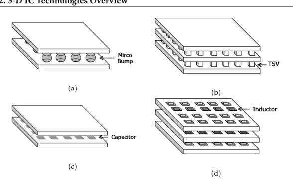
(25) 1.2. 3-D IC Technologies Overview voltage-drop [23] [36]. Second, BEOL metal and via are the key to make scaling improvement. Single pattering is limited to metal pitch around 90nm in ultraviolet light 193nm immersion lithography [34]. Although layout-friendly double/triple patterning techniques can be adopted to further reduce the metal pitch, greater RC variation [37], additional process cost, and increasing design complexity must be specially taken care and required closely collaboration between design houses and foundries [34]. Third, the idea of three-dimensional (3-D) integrated circuit (IC) technology is one of promising solution in facing the ultimate physical challenges. 2.5-D through-silicon-via (TSV)/interposer has been proven its feasibility from homogeneous to heterogeneous multi-die stacking [38] [34] [1] [2]. However, to stack heterogeneous ICs with TSV technology in real 3-D style still remains challenges and requires to go through more researching processes. In recent years, wireless inductive 3-D integration technologies also draw a lot of attention in offering cost-effective, reliable, and scalable solutions [35].. 1.2 3-D IC Technologies Overview As transistor process technology continues shrinking, not only is the manufacturing technology facing increasing challenges in physical design, but also the capital cost of semiconductor manufacture skyrockets. To pursue the Moores law, the emerging three dimensional integrated circuit technologies offer viable. 8.
(26) 1.2. 3-D IC Technologies Overview. (a). (b). (c). (d). Figure 1.5: 3-D inter-chip interconnection technologies (a) Micro-Bump (b) Through-Silicon-Via (TSV) (c) Capacitive-Coupling Interface (d) InductiveCoupling Interface. solutions and have attracted significant attention in recent years. The 3-D chips stacking interface can be classified into wired and wireless interfaces. This section reviews wired and wireless approaches and introduces the basic concept of inductive coupling interface.. 1.2.1 Wired 3-D Interface • Wire bonding is the method of making interconnection between chips in die-level. It is widely used in system-in-package (SiP) and is considered the most cost-effective and flexible interconnect technology. Nevertheless, wire bonding interconnects density is limited to <400/mm2 pitch [6] due to its long bonding wires and electrostatic-discharge (ESD) protection devices.. 9.
(27) 1.2. 3-D IC Technologies Overview As the result, not only is the inter-chip wiring delay considerable, but also its communication bandwidth is bounded. • Micro-bump is a die-level interconnection technology. It utilizes solder balls formed on the chip surface to stack dies by face-to-face and is illustrated in Figure 1.5 (a). In recent years, the microbump interconnection technology is also extended to enable 2.5-D chips integration [1–3]. That is, heterogeneous chips can be mounted on silicon interposer by joining microbumps. The silicon interposer can offer signal routing resource for inter-chips and package interconnections. • Through-silicon-via (TSV) is a wafer-level interconnection technology. That is, the formation of inter-die vias occur when the fabrication processes is taking place. Figure 1.5 (b) depicts the overview of TSV based ICs stacking. TSV can completely pass through a silicon wafer and hence more than two chips can be connected by face-to-back stacking. Additionally, because its electrical properties, resistance, capacitance, and parasitic inductance, are better than wire bonding and TSV footprint is also comparably smaller, TSV can lead to higher performance, offer higher communication bandwidth, and lower power consumption [4,31]. However, TSV technologies have various issues in yield and cost due to stacking misalignment, chip bending under thermal stress, 3r d party chip integration, die testing, thermal concerns, and commercial availability of electronic design automation (EDA) tools [7, 32].. 10.
(28) 1.2. 3-D IC Technologies Overview For several years, the semiconductor industry has been talking about the development of 2.5-D and 3-D chips using wiring solution, TSV. Although there is progress in 3-D IC research in recent years, there are still yield and cost issues in TSV solution. It must be noted that manufacturing yield can drop below 40% easily even if TSV yield can achieve 99.99% and thus TSV yield recovery circuit overhead is required [49]. Moreover, it is also reported that 3-D TSV technology adds 15% or more in wafer processing cost in comparing to traditional planar flow. Regarding 2.5-D solution, the interposer requires additional 25% or more to the silicon cost before packaging [26]. As a result, 2.5-D and 3-D chips are currently only adopted in high-end applications, such as FPGA and GPU [27]. And generally, the TSV solutions are still too expensive for cost-sensitive mobile SoC at least for now.. 1.2.2 Wireless 3-D Interface • Capacitive-coupling interface is a die-level wireless interconnection technology. Capacitive coupling interface utilizes electric field change between two metal plates to transmit data [8–11]. Figure 1.5 (c) illustrates the capacitive coupling based face-to-face ICs stacking. Since capacitive coupling interface is voltage-driven, it has limitation in transmitting data for long distance in following voltage-scaling trend [12]. Its communication distance is limited to few microns and it is only achievable in the face-to-face stacking.. 11.
(29) 1.3. ThruChip Interface Technology Overview Therefore, the capacitive coupling interface technology is limited to a stack of two chips. • Inductive-coupling interface is also a die-level wireless interconnection and is also called ThruChip Interface (TCI). TCI transmit and receive data signals through magnetic flux change between on-chip coils. The idea of TCI has been researched in diverse 3-D IC applications [13–17]. Figure 1.5 (d) shows an example of inductive coupling based face-to-back ICs stacking. Because the inductive coils are implemented with common metal layers, no additional fabrication process is needed. In contrast to capacitive-coupling interface, TCI is current-driven and thus the transmit power can be increased even at low voltages in scaled devices. Its communication distance can range from few microns to hundred microns and face-to-back stacking is possible.. 1.3 ThruChip Interface Technology Overview Since 2004, research on wireless 3-D interconnection interface, ThruChip Interface (TCI), were presented every year in various IC applications in International Solid-State Circuits Conference (ISSCC). TCI showed its advantages of flexibility, cost (20$/chip), comparable data rate (10Gb/s/ch) [17], communication reliability (BER <10−14 ), and energy dissipation (0.14pJ/b) [16]. Although TCI is wireless data communication interface, however, it does not need to deal with. 12.
(30) 1.3. ThruChip Interface Technology Overview sophisticated communication mechanism. That is, a set of RF circuits, such as passive filter, mixer, amplifier, frequency synthesizer, and etc., is not required to sustain signal-to-noise ratio (SNR) and raise communication bandwidth. Since TCI is utilized in proximal communication (10um-1.2cm), its architecture can be comparably simple. Figure 1.6 illustrates the simplified TCI circuit diagram and its operation scheme. The basic principle of TCI communications is magnetic induction. The TCI transmitter circuit can be a simple H-bridge driver circuit which can vary transmit current, IT X , through transmitter coil to create magnetic field variation (H) in the vicinity. The change of magnetic field is proportional to the change rate of IT X , dIT X /dt. When the varying magnetic field arrive the receiver coils on adjacent layers, an induced current will be generated to reduce the change of magnetic field and thus a corresponding electromotive force, VR , will appear. The relationship between VR and dIT X /dt can be formulated as. VR (t) = M. dIT X (t) dt. (1.3.1). where M is the mutual inductance between transmitter and receiver coils. The receiver circuit can be a hysteresis comparator to sense the small pulse, VR , and convert it to digital data. Due to its wireless nature, TCI based chips can be added, removed, updated in hardware modules easily even after chips are stacked. Furthermore, TCI based chips are allowed to test for good dies through contact-less interface. On the. 13.
(31) 1.4. TCI Design Automation Issues. Figure 1.6: Basic ThruChip Interface (TCI) architecture and its operation diagram [17]. contrary, wiring 3-D IC stacking solution, such as through-silicon-via (TSV), has known-good-dies (KGD) issues. Hence, it can be seen that TCI is cost-effective in the perspectives of yield, fabrication, and testing in comparison with wiring solution and thus considered one of emerging 3-D interconnection technology.. 1.4 TCI Design Automation Issues Unlike conventional wiring interconnection that designer has complete integrated tools and explicit design guideline, TCI relies on electromagnetic pulse to communicate from layers to layers and there is no dedicated EDA tools available. Hence, there are some learning curves that circuit designers must go through. 14.
(32) 1.4. TCI Design Automation Issues before adopting TCI in their design. To boost TCI design automation development, three TCI design automation topics, physical design consideration, inductive coupling channel optimization, and timing and noise optimization in reconfigurable system, are addressed.. 1.4.1 Physical Design Considerations Since TCI is supposed to utilize in diverse 3-D IC applications, the eddy current impacts in common physical design structures, such as power mesh and dummy metal fill, still do not be explored in TCI communication. Especially, mesh style power distribution network (PDN) is inevitable in high performance (power) circuit designs. Because TCI coils usually occupy a considerable layout area, it is preferable to place logic gates beneath the TCI coils for better area utilization. As a result, without the design guidelines, designers may have to put TCI in a comparable conservative physical environment to avoid fail chip. It does not only waste routing resource but also make TCI less attractive in stacking chip technology.. 1.4.2 Inductive Coupling Channel Optimization Regarding the conventional TCI design flow, to design inductive coupling channel is one of timing consuming task. Circuit designers usually have to spend a couple of days in trial-and-error adjust spiral inductor coil layout parameters to find an acceptable inductive coupling solution. Moreover, the quality of in-. 15.
(33) 1.4. TCI Design Automation Issues ductive coupling channel directly reflect on TCI communication. That is, a good inductive coupling channel does not only ensure communication reliability but also directly reduce power consumption. Therefore, it is better to find an optimal solution instead of using fair solutions.. 1.4.3 Timing Optimization and Noise Avoidance in 3-D FPGA System Conventionally, FPGA research topics tend to focus on improving its capacity, performance, and architecture complexity. In the high-end FPGAs applications, FPGAs are usually adopted in communication infrastructure, advanced radar, medical applications, machine vision, ASIC emulation/prototype, and suchlike. FPGA rarely appears in consumer or hand-held products. In 2014, ACM/SIGDA International Symposium on Field-Programmable Gate Arrays raised the topic on FPGA for mobile applications for the first time [28]. New FPGA technologies have started to emerge to comprise small footprint, low cost, and extreme low power consumption(50 µW) and made FPGA suitable for diverse mobile applications [29]. However, because the size of mobile device is usually limited, the size of mobile FPGA can not be designed too large and thus its capacity is bound. Instead of increasing capacity by enlarging FPGA die size, it can be extended by stacking FPGAs in 3-D. Since TSV solutions are still too expensive for consumer mobile applications at least for now, TCI can be an alternative solution. Nevertheless,. 16.
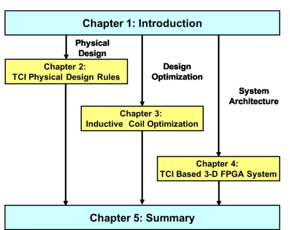
(34) 1.5. Thesis Organization because TCI usually needs to consume considerable metal layout footprint, the adoption of time-division-multiplexing (TDM) technique is required to fully utilize its bandwidth and achieve better layout area utilization. On the other hand, because the TCI signal routing through TDM scheme is different to conventional wiring routing, TDM timing slot rescheduling scheme is required to assign TDM timing slot to optimize vertical routing delay. Additionally, since electromagnetic waves may propagate through several stacked chips and cause signal interference issues, the electromagnetic noise must be specially taken care while assigning timing slots. Therefore, when TCI is adopted in a complex reconfigurable network routing structure, an electromagnetic interference avoidance scheme is required to reduce the possibility of inter-layer signal interference. Figure 1.7 illustrates the overview of TCI based 3-D FPGA system that this thesis is going to explore.. 1.5 Thesis Organization Although researches in TCI have lasted for years, few researches focus on discussing its design automation and optimization. This does not only make its learning curve steep but also hinder it from widely adopting. The purpose of this thesis is to discuss TCI design automation topics in physical design consideration, inductive coupling channel optimization, timing optimization and noise avoidance technique in reconfigurable system to enrich TCI design guidelines. Since the topics of this thesis cover TCI design automation from system architecture. 17.
(35) 1.5. Thesis Organization. Figure 1.7: Overview of TCI based 3-D FPGA architecture [41]. implementation to physical design and the perspectives of TCI design automation are extensive, to avoid confusion, the chapters of this thesis are organized in bottom up order and each chapter is independent. In Chapter 2, three TCI physical design rules, the dependence between power consumption and coil dimension to communication distance ratio, power mesh impact, and dummy metal impact, are presented and analyzed with test chip measurement and various field-solver simulations. Although power mesh impact on TCI has been explored in previous work [47], it did not has in-depth exploration in formation of eddy current and discuss solutions in suppressing eddy current on power mesh. In this chapter, a TCI design methodology is proposed to effectively suppress eddy current on power mesh with only minor impact on. 18.
(36) 1.5. Thesis Organization. Figure 1.8: The thesis organization. power mesh structure. In Chapter 3, an analytical inductive coupling channel design automation flow is introduced. Though there is already a geometric programming (GP) based spiral inductor optimization methodology [48], its both objective and subjective equations are limited to posynomial functions and additional curve fitting steps are required to transform non-posynomial equations. The proposed design automation flow can not only help designer reduce their time in searching acceptable inductive coupling solution from days to minutes but also provide a platform to enable designers to explore the trade-off in TX/RX coil configurations.. 19.
(37) 1.5. Thesis Organization Moreover, the proposed flow can find optimal inductive coupling solution and raise 17% mutual inductance value improvement on average in comparing to previous works. The spice simulation results also show 16.8% average power reduction in comparing to the previous work [42]. In Chapter 4, a novel TCI based 3-D FPGA architecture exploration framework is addressed. Although the idea of 3-D FPGA is not new and has been proven with real chip in multi-chips module (MCM) stacking [39] and architecture evaluations [40] [4], the stacking cost and yield make it far from reality and impede its further development. Moreover, since FPGA is supposed to apply in diverse applications and it is reported that 70% FPGA area is used by routing resources and 80% delay is also contributed from routing resources [18]. It can be seen that a good 3-D IC stacking interface for FPGA shall at least have two primary characteristics, high communication bandwidth and low assembling cost. Because TCI is wireless interface (no yield loss during stacking) and can provide high communication bandwidth, a TCI based 3-D FPGA architecture framework is developed to explore its trade-off in performance and area overhead. This chapter also discusses the foreseeable issues while adopting TCI in reconfigurable system and offers effective solutions in TCI routing and timing optimization. A reconfigurable TCI block area estimation methodology and a TCI timing division multiplexing (TDM) timing slot optimization algorithm are also introduced. The experimental results show the proposed 3-D FPGA architecture can reduce delay by 25% on average and 58% at maximum over 2-D FPGA. 20.
(38) 1.5. Thesis Organization in predictive technology model (PTM) [43]. Although the performance of TCI based 3-D FPGA architecture is 8% less than through-silicon-via (TSV) based 3D FPGA on average, TCI based architecture can reduce active area consumed by vertical communication channels by 42% on average and hence get better area and delay product. In Chapter 5, a conclusion of this dissertation is drawn and a potential future study is also discussed.. 21.
(39) References for Chapter 1 [1] L. Madden, E. Wu, N. Kim, B. Banijamali, K. Abugharbieh, S. Ramalingam, and X. Wu, ”Advancing high performance heterogeneous integration through die stacking,” IEEE Proceedings of the ESSCIRC, Bordeaux, Sept. 2012, pp. 18-24. [2] A. Rahman, J. Schulz, R. Grenier, K. Chanda, M.J. Lee, D. Ratakonda, H. Shi, Z. Li, K. Chandrasekar, J. Xie, and D. Ibbotson, ”Interconnection requirements and multi-die integration for FPGAs,” IEEE International Interconnect Technology Conference (IITC), Kyoto, Jun. 2013, pp. 1-3. [3] L. Madden, E. Wu, N. Kim, B. Banijamali, K. Abugharbieh, S. Ramalingam and X. Wu, ”Advancing high performance heterogeneous integration through die stacking,” in Proceeding ESSCIRC, 17-21 Sept., 2012, pp. 18-24. [4] C. Ababei, H. Mogal, and K. Bazargan, ”Three-dimensional place and route for FPGAs,” IEEE Trans. on CAD, Jun., 2006, Vol. 25, Issue 6, pp. 1132-1140.. 22.
(40) REFERENCES FOR CHAPTER 1 [5] K. Siozios, K. Sotiriadis, V. F. Pavlidis, and D. Soudris, ”Exploring alternative 3D FPGA architectures: design methodology and CAD tool support,” in Int. Conf. FPL, Aug. 2007, pp. 652-655. [6] K. C. Saraswat, ”3-D ICs: motivation, performance analysis, technology and application,” IEEE Int. Symp., IPFA, 5-9 Jul. 2010, pp. 1-6. [7] J. H. Lau, ”TSV manufacturing yield and hidden costs for 3D IC integration,” in Proceeding ECTC, 1-4 Jun. 2010, pp. 1031-1042. [8] Q. Gu, Z. Xu, J. Ko, and M.-C. F. Chang, ”Two 10Gb/s/pin low-power interconnect methods for 3D ICs,” IEEE International Solid-State Circuits Conference (ISSCC), Digest of Technical Papers, San Francisco, CA, Feb. 2007, pp. 448-449. [9] K. Kanda, D. D. Antono, K. Ishida, H. Kawaguchi, T. Kuroda, and T. Sakurai, ”1.27Gb/s/pin 3mW/pin wireless superconnect (WSC) interface scheme,” IEEE International Solid-State Circuits Conference (ISSCC), Digest of Technical Papers, San Francisco, CA, Feb. 2003, pp. 186187. [10] R. J. Drost, R. P. Hopkins, and I. E. Sutherland, ”Proximity communication,” in Proceeding CICC, Sep. 2003, pp. 469472. [11] A. Fazzi, R. Canegallo, L. Ciccarelli, L. Magagni, F. Natali, E. Jung, P. L. Rolandi, and R. Guerrieri, ”3D Capacitive Interconnections with Mono- and Bi-Directional Capabilities,” IEEE International Solid-State Circuits Confer-. 23.
(41) REFERENCES FOR CHAPTER 1 ence (ISSCC), Digest of Technical Papers, San Francisco, CA, Feb. 2007, pp. 356-357. [12] N. Miura, D. Mizoguchi, T. Sakurai, and T. Kuroda, ”Analysis and design of inductive coupling and transceiver circuit for inductive inter-chip wireless superconnect,” IEEE JSSC, Vol. 40, No. 4, Apr. 2005, pp. 829-837. [13] Y. Sugimori, Y. Kohama, M. Saito, Y. Yoshida, N. Miura, H. Ishikuro, T. Sakurai, and T. Kuroda, ”A 2Gb/s 15pJ/b/chip inductive-coupling programmable bus for NAND flash memory stacking,” IEEE International Solid-State Circuits Conference (ISSCC), Digest of Technical Papers, San Francisco, CA, Feb. 2009, pp. 244-245. [14] H. Ishikuro, T. Sugahara, and T. Kuroda, ”An attachable wireless chip access interface for arbitrary data rate using pulse-based inductive-coupling through LSI package,” IEEE International Solid-State Circuits Conference (ISSCC), Digest of Technical Papers, San Francisco, CA, Feb. 2007, pp. 360361. [15] N. Miura, Y. Kohama, Y. Sugimori, H. Ishikuro, T. Sakurai, and T. Kuroda, ”A high-speed inductive-coupling link with burst transmission,” IEEE JSSC, vol. 44, no. 3, Mar. 2009, pp. 947-954. [16] N. Miura, H. Ishikuro, T. Sakurai, and T. Kuroda, ”A 0.14pJ/b inductivecoupling inter-chip data transceiver with digitally-controlled precise pulse. 24.
(42) REFERENCES FOR CHAPTER 1 shaping,” IEEE International Solid-State Circuits Conference (ISSCC), Digest of Technical Papers, San Francisco, CA, Feb. 2007, pp. 358-359. [17] N. Miura, Y. Kohama, Y. Sugimori, H. Sakurai, and T. Kuroda, ”An 11Gb/s inductive-coupling link with bust transmission,” IEEE International SolidState Circuits Conference (ISSCC), Digest of Technical Papers, San Francisco, CA, Feb. 2008, pp. 298-299. [18] V. Betz, J. Rose, and A. Marquardt, ”Architecture and CAD for DeepSubmicron FPGAs,” Springer, 1999. [19] S.H. Yang, J.Y. Sheu, M.K. Ieong, M.H. Chiang, T. Yamamoto, J.J. Liaw, S.S. Chang, Y.M. Lin, T.L. Hsu, J.R. Hwang, J.K. Ting, C.H. Wu, K.C. Ting, F.C. Yang, C.M. Liu, I.L. Wu, Y.M. Chen, S.J. Chent, K.S. Chen, J.Y. Cheng, M.H Tsai, W. Chang, R. Chen, C.C. Chen, T.L. Lee, C.K Lin, S.C. Yang, Y.M. Sheu, J.T. Tzeng, L.C. Lu, S.M Jang, C.H. Diaz, and YJ Mii, ”28nm metal-gate highK CMOS SoC technology for high-performance mobile applications,” IEEE Custom Integrated Circuits Conference (CICC), San Jose, CA, Sept. 2011, pp. 1-5. [20] D. Hisamoto, W.-C. Lee, J. Kedzierski, H. Takeuchi, K. Asano, C. Kuo, E. Anderson, T.-J. King, J. Bokor, and C. Hu, ”FinFET-a self-aligned doublegate MOSFET scalable to 20 nm,” IEEE Transactions on Electron Devices, Vol. 47, Issue 12, Dec. 2000, pp. 2320-2325.. 25.
(43) REFERENCES FOR CHAPTER 1 [21] C. Hu, ”New sub-20nm transistors why and how,” IEEE Design Automation Conference (DAC), New York, NY, June 2011, pp. 460-463. [22] ”16nm Technology,” [Online]. Available: http://www.tsmc.com/english/dedicatedFoundry/technology/16nm.htm [23] G. Yeap, ”Smart mobile SoCs driving the semiconductor industry: technology trend, challenges and opportunities,” in IEEE International Electron Devices Meeting (IEDM), Washington, DC, Dec. 2013, pp. 1.3.1-1.3.8. [24] https://www.idc.com/ [25] H. Jones, ”White paper: why migration to 20nm bulk CMOS and 16/14nm FinFETs is not best approach for semiconductor industry,” International Business Strategies (IBS), Jan. 2014. [Online]. Available: http://www.soitec.com/pdf/WP handel-jones.pdf [26] M. Lapedus, ”Time to revisit 2.5D and 3D” [Online]. Available: http://semiengineering.com/time-to-revisit-2-5d-and-3d/ [27] ”High bandwidth memory” [Online]. Available: http://www.amd.com/en-us/innovations/software-technologies/hbm [28] M. Maxfield, ”First time ever at ACM/SIGDA conference: FPGAs for mobile apps,” EEtimes, Feb. 2014. [Online]. Available: http://www.eetimes.com/document.asp?doc id=1321063. 26.
(44) REFERENCES FOR CHAPTER 1 [29] ”An FPGA approach to implementing time-critical functions in multisensor mobile designs,” Lattice Semiconductor White Paper, Jul. 2013. [30] Z. Or-Bach, ”28nm: The Last Node of Moore’s Law,” EEtimes, Mar. 2014. [Online]. Available: http://www.eetimes.com/author.asp?doc id=1321536 [31] Sung Kyu Lim, ”Design for high performance, low power, and reliable 3D integrated circuits,” Springer, 2012. [32] A. Papanikolaou, D. Soudris, and R. Radojcic, ”Three dimensional system integration: IC stacking orocess and design,” Springer, 2011. [33] K. Zhang, ”Memory 2014 trends,” in ISSCC Tech Trends, 2014,pp. 29-30. [34] J.Y.-C. Sun ”System scaling and collaborative open innovation,” IEEE VLSI Technology Symposium (VLSIT), Kyoto, Jun. 2013, pp. T2-T7. [35] T. Kuroda, ”ThruChip interface (TCI) for 3D networks on chip,” IEEE International Conference on VLSI and System-on-Chip (VLSI-SoC), Hong Kong, Oct. 2011, pp. 238-241. [36] C. Forzan and D. Pandini, ”Why we need statistical static timing analysis,” IEEE International Conference on Computer Design (ICCD), Lake Tahoe, CA, Oct. 2007, pp. 91-96. [37] P. Evanschitzky, A. Burenkov, and J. Lorenz, ”Double Patterning: Simulating a Variability Challenge for Advanced Transistors,” IEEE International Con-. 27.
(45) REFERENCES FOR CHAPTER 1 ference on Simulation of Semiconductor Processes and Devices (SISPAD), Glasgow, Sept. 2013, pp. 105-108. [38] W.C. Chiou, K.F. Yang, J.L. Yeh, S.H. Wang, Y.H. Liou, T.J. Wu, J.C. Lin, C.L. Huang, S.W. Lu, C.C. Hsieh, H.A. Teng, C.C. Chiu, H.B. Chang, T.S. Wei, Y.C. Lin, Y.H. Chen, H.J. Tu, H.D. Ko, T.H. Yu, J.P. Hung, P.H. Tsai, D.C. Yeh, W.C. Wu, A.J. Su, S.L. Chiu, S.Y. Hou, D.Y. Shih, Kim H. Chen, S.P. Jeng and C.H. Yu, ”An ultra-thin interposer utilizing 3D TSV technology,” IEEE Symposium on VLSI Technology (VLSIT), Honolulu, HI, Jun. 2012, pp. 107-108. [39] M. J. Alexander, J. P. Cohoon, J. L. Colflesh, J. Karro, and G. Robins, ”ThreeDimensional Field-Programmable Gate Arrays,” IEEE Proceeding International ASIC Conference, 1995, pp. 253-256. [40] M. J. Alexander, J. P. Cohoon, J. L. Colflesh, J. Karro, E. L. Peters, and G. Robins, ”Placement and Routing for Three-Dimensional FPGAs,” IEEE Proceeding 4th Canadian Workshop Field-Programmable Device, Toronto, ON, Canada, 1996, pp. 11-18. [41] L.-C. Hsu, M. Motomura, Y. Take, and T. Kuroda, ”Through Chip Interface Based Three-Dimensional FPGA Architecture Exploration,” IEICE Transaction, Vol. E98-C, No. 4, Apr. 2015, pp. 288-297. [42] L.C. Hsu, Y. Take, A. Kosuge, S. Hasegawa, J. Kadomoto, and T. Kuroda, ”Design and analysis for ThruChip design for manufacturing (DFM),” IEEE. 28.
(46) REFERENCES FOR CHAPTER 1 Design Automation Conference Asia and South Pacific (ASP-DAC), Chiba, Japan, 2015, pp. 46-47. [43] W. Zhao and Y. Cao, ”New generation of Predictive Technology Model for sub-45nm early design exploration,” IEEE Transaction on Electron Devices, Nov. 2006, vol. 53, no. 11, pp. 2816-2823. [44] T. Song, W. Rim, J. Jung, G. Yang, J. Park, S. Park, K.-H. Baek, S. Baek, S.K. Oh, J. Jung, S. Kim, G. Kim, J. Kim, Y. Lee, K. S. Kim, S.-P. Sim, J. S. Yoon, and K.-M. Choi, ”13.2 A 14nm FinFET 128Mb 6T SRAM with VMINenhancement techniques for low-power applications,” IEEE International Solid-State Circuits Conference (ISSCC), Digest of Technical Papers, San Francisco, CA, Feb. 2014, pp. 232-233. [45] D. Payne, ”Designing with FinFETs,” [Online]. Available: https://www.semiwiki.com/forum/content/1709-designing-finfets.html [46] Zvi Or-Bach and B. Louie, ”The most expensive SRAM in the world 2.0,” [Online]. Available: http://electroiq.com/blog/2014/02/the-most-expensive-sram-in-theworld-2-0/ [47] K. Osada, M. Saen, Y. Okuma, K. Niitsu, Y. Shimazaki, Y. Sugimori, Y. Kohama, K. Kasuga, I. Nonomura, N. Irie, T. Hattori, A. Hasegawa, and T. Kuroda, ”3D system integration of processor, multi-stacked SRAMs by us-. 29.
(47) REFERENCES FOR CHAPTER 1 ing inductive-coupling links,” IEEE VLSI Circuits Symposium, Kyoto, Jun. 2009, pp. 256-257. [48] M. del Mar Hershenson, S.S. Mohan, S.P. Boyd, and T.H. Lee, ”Optimization of inductor circuits via geometric programming,” IEEE Design Automation Conference, New Orleans, LA, Jun. 1999, pp. 994-998. [49] A.-C. Hsieh and T.-T. Hwang, ”TSV redundancy: architecture and design issues in 3-D IC,” IEEE Transaction on VLSI Systems, Apr. 2012, vol. 20, No. 4, pp. 711-722.. 30.
(48) Chapter 2 ThruChip Physical Design Guideline Exploration. 31.
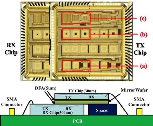
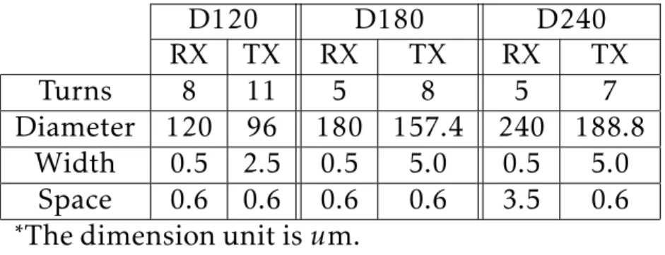
(49) 2.1. TCI Design Guideline Exploration. 2.1 TCI Design Guideline Exploration TCI can offer an alternative and cost-effective solution in 3-D IC stacking. However, some physical design considerations still remain mysterious and are worthwhile to explore. To examine the TCI constraints in physical design, a test chip is first designed and fabricated in TSMC 0.18um CMOS technology to explore the TCI physical design guidelines. Figure 2.1 illustrates the test chip microphotograph and its cross-section configuration view. Two chips are stacked by face-to-back. The top chip is thinned to 30um and the bottom chip is kept 300um. The thickness of glue layer is about 5um. A mirror wafer is placed between two chips and its thickness ranges from 30um to 100um to provide various communication distances. Three TCI design scenarios, Fig. 2.1 (a), (b), and (c), are prepared in this test chip. Each TCI coil is extended and protected by ground shield to reduce capacitive-coupling noise from surrounding logic signals [1]. In Fig. 2.1 (a), three kinds of coil pairs, D240, D180, and D120, where D means outer coil dimension and the following number means size, are deployed as baseline scenarios. Table 2.1 shows the detail configurations of D240, D180, and D120 coil pairs. In baseline scenarios, the space between transmitter (TX) and receiver (RX) coils is kept clear. These baseline coil pairs are not only the benchmark for other scenarios but also used to evaluate design guideline in determination of coil size scaling trend over wafer thinning. The communication distance varies from 70um to 140um in chips assembling.. 32.
(50) 2.1. TCI Design Guideline Exploration. Figure 2.1: Test chip microphotograph and chips stacking cross-section view (a) Baseline (b) Dummy metal scenario (c) Power mesh scenario.. 33.
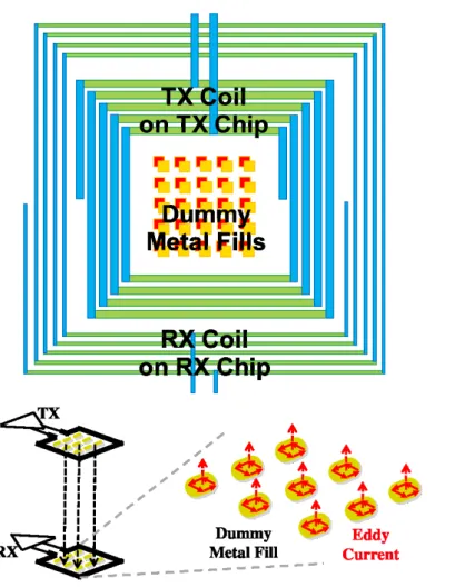
(51) 2.1. TCI Design Guideline Exploration Table 2.1: The detail configurations of TX and RX coil pairs.. D120 D180 RX TX RX TX Turns 8 11 5 8 Diameter 120 96 180 157.4 Width 0.5 2.5 0.5 5.0 Space 0.6 0.6 0.6 0.6 ∗ The dimension unit is um.. D240 RX TX 5 7 240 188.8 0.5 5.0 3.5 0.6. The second design guideline exploration is related to power mesh. Although power mesh impact has been discussed in [2] and additional transmitting power requirement is observed to compensate the eddy current impact, the power mesh used in [2], however, is not general in high performance ASIC design. To evaluate the power mesh impact in extreme case, a high density power meshes are placed between TCI coil pairs, D240, D180, and D120. They are shown in Fig. 2.1 (c). The power/ground line width is set to 16um and the space between two lines is set to 4um. The power mesh is drawn by METAL5 and METAL6. Figure 2.2 (a) shows an example of power mesh scenario layout and (b) illustrates how the eddy current will be formed on the power mesh when TCI is activated. The third topic of design guideline is about dummy metal fill impact exploration. In this scenario, there are three different densities, 20%, 50%, and 80%, dummy metal fill arrays placed within D240 coil pairs and they are shown in Fig. 2.1 (b). The arrays of floating dummy fill consist of metal layers from one to six. Figure 2.3 (a) depicts one layout example of dummy metal fill scenario and. 34.
(52) 2.2. Measurement Results and Design Analysis (b) shows how the eddy current may arise on the dummy metal shreds.. Figure 2.2: (a) The top-bottom layout view of the power mesh scenario. The power mesh is on the RX Chip. (b) Illustration of induced eddy current on power mesh.. 2.2 Measurement Results and Design Analysis 2.2.1 The Baseline Scenarios In the test chip measurement, each TCI channel was set to operate at data rate 1Gb/s. The bit error rate (BER) was recorded by sweeping transmitting power.. 35.
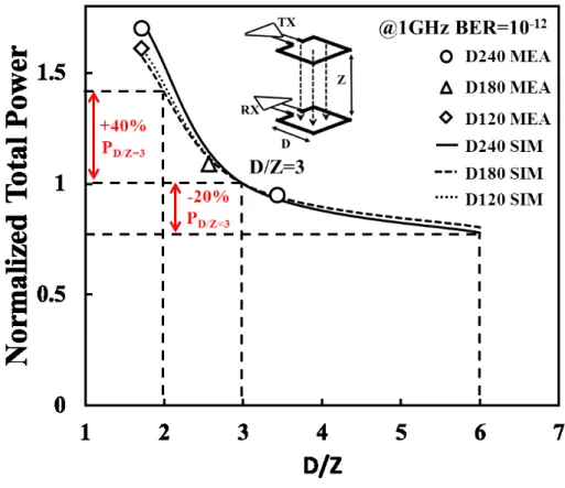
(53) 2.2. Measurement Results and Design Analysis. Figure 2.3: (a) The top-bottom layout view of the dummy metal fill scenario. The dummy metal fill is deployed on both chips. (b) Illustration of induced eddy current on dummy metal fill. Figure 2.4 depicts the BER dependence on transmit power in baseline scenarios. Figure 2.5 illustrates the relation between D/Z and normalized total power in both measurement and simulation data. The total power is normalized to the total power of D/Z=3 simulation result. It can be seen that designing TCI coil by following D/Z=3 rule is the most efficient and nearly optimal. If the power consumption is the major concern, enlarging coil size or reducing the wafer thickness. 36.
(54) 2.2. Measurement Results and Design Analysis. Figure 2.4: Bit Error Rate (BER) vs. Transmitting Power[mW].. 37.
(55) 2.2. Measurement Results and Design Analysis can further reduce TCI power consumption. Nevertheless, the power reduction efficiency of reducing power by increasing D/Z ratio is not so excited. Figure 2.5 shows that increasing D/Z ratio to 6 can only reduce power consumption by 20%. On the other hand, when D/Z is reduced to 2, 40% additional power is required to sustain the communication reliability.. Figure 2.5: Normalized Total Power vs. D/Z in both measurement and simulation results.. 38.
(56) 2.2. Measurement Results and Design Analysis. 2.2.2 The Power Mesh Impact Regarding power mesh experiment, we are unable to measure any data from receiver side even if we push the transmitting power to the maximum value. The condition can also be observed in field solver and spice simulations. Figure 2.6 illustrates the current density maps created by field solver simulation at 1 GHz. Figure 2.6 (a) represents the condition that a high-density power mesh is placed between TX and RX coils. The current density map indicates that the eddy current on the power mesh consumes the majority of the magnetic pulse energy and only few induced current appears on the RX coil. The induced eddy current is especially strong near the TCI coils. If only power stripes are placed between TX and RX coils, we can see that coupling current can still be induced on the RX coil and it is shown in Fig. 2.6 (b). The phenomenon is identical to [2]. That is, metal stripes have no impact on TCI transmission and eddy current on the conductive loop will degrade the TCI capability. In order to analyze how the eddy current affects the coupling coefficient, we perform a set of field-solver simulations to see the relation between conductive loops and TCI RX coils. The conductive loop is pushed away by removing stacked power via within X, where X is the distance between the conductive loop and RX coil. Figure 2.7a shows the simulation results in the form of normalized coupling coefficient versus X/D ratio, where D is the outer coil dimension. Since the induced voltage, VR , on the RX coil is proportional to coupling coefficient, K, it can be seen that additional transmitting power is required to compensate the loss of. 39.
(57) 2.2. Measurement Results and Design Analysis. (a) Current density map in power mesh scenario.. (b) Current density map in power stripes only scenario.. Figure 2.6: Illustration of current density map in power mesh and power stripes only scenarios (a) The induced eddy current on the conductive loops forming on the power mesh will consume most of the magnetic pulse energy and thus cause RX coil fail to sense the magnetic signal (b) Most of the magnetic pulse can reach RX coil if there are power stripes only (no formation of conductive loops) between TX and RX coils.. 40.
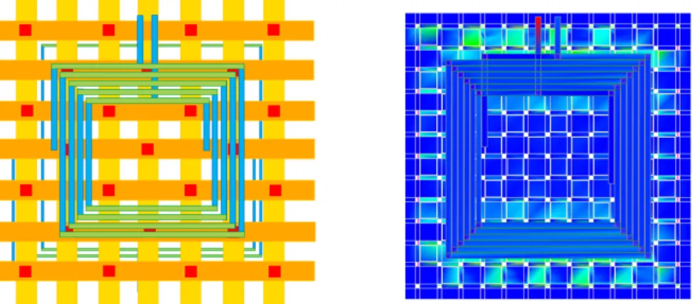
(58) 2.2. Measurement Results and Design Analysis K value. However, because transmitting power is bounded by device physical characteristics, there exists a coupling coefficient threshold, Kth , which must be kept while designing TCI. If K drops below Kth , the TCI will fail to sustain acceptable communication reliability and power consumption. Figure 2.7 (b) and (c) indicate how the eddy current finds its shortest path when X/D equals 0.25 and 0.9 respectively. From these figures, we can see that the induced eddy current is strong when the formed conductive loop is closed to RX coil. If the eddy current can be guided away from TCI coils, the effect of eddy current can become weaker and thus the coupling coefficient can be recovered. Removing stacking power vias to recover K value is not so practical in real design because it is too aggressive become power mesh structure. To minimize the power mesh structure impact and recover coupling coefficient efficiently, a method of creating a minimum space gap on power lines to guide eddy current away is proposed. Figure 2.8a illustrates the basic idea and its recovery efficiency in comparison to removing power vias in D240 scenario. Figure 2.8 (b) and (c) show how the induced eddy current is guided away from inductive coupling coils in X/D=0.25 and X/D=0.9 respectively. To evaluate the power mesh structure impact of the proposed coupling coefficient recovery method in LSI design, we realized a microprocessor, OpenCore [3], design with place and routing tool [4] in TSMC 180nm technology. The core size is 700um x 700um and the cell utilization ratio is about 80%. To simply the the voltage drop evaluation work, only TCI coils are placed in the OpenCore. 41.
(59) 2.2. Measurement Results and Design Analysis. (a) Normalized Coupling Coefficient (K) Vs. X/D (D120, D180, and D240).. (b) X/D=0.25 (D240). (c) X/D=0.9 (D240). Figure 2.7: Recover coupling coefficient (K) by removing stacked power vias to guide eddy current away from TCI coil. (a) Normalized Coupling Coefficient (K) Vs. X/D (D120, D180, and D240) (b) Eddy current density map when X/D=0.25 (c) Eddy current density map when X/D=0.9. 42.
(60) 2.2. Measurement Results and Design Analysis. (a) Normalized Coupling Coefficient (K) Vs. X/D (D240).. (b) Current Density Map (X/D=0.25, D240).. (c) Current Density Map (X/D=0.9, D240).. Figure 2.8: Recover coupling coefficient (K) by creating a minimum space gap on power mesh lines to guide eddy current away from TCI coil.. 43.
(61) 2.2. Measurement Results and Design Analysis design and the integration work of OpenCore design and TCI circuit is further discussed in Appendix A. Figure 2.9 shows the dynamic IR-drop heat-map analysis in baseline, stacking power vias removal, and power mesh minimum space splitting scenarios. It can be seen that the IR-drop heat maps of both baseline and the proposed K recovering methodology are similar. Figure 2.10 shows the dynamic IR-drop ratio versus X/D ratio. The maximum IR-drop value in baseline case is 6.5%. From Figure 2.10, we can see that the proposed method only causes additional 0.5% IR-drop when X/D equals 0.9 (77% K value recovery). To further study the voltage-drop impact in multi-coil scenario, four D120 coils are placed in the OpenCore design with minimum space chop technique. Figure 2.11 (a) and (b) illustrate the heat maps in one D240 coil pair and four D120 coil pairs with minimum space chop technique applied respectively. The X/D ratios in these two cases are set to 0.9. Figure 2.11 (c) shows the IR-drop histogram of these two scenarios. The minimum space chop in the four D120 coil scenario introduces additional 0.4% to the maximum voltage-drop in comparing to the single D240 coil case. Furthermore, from Figure 2.11, it can also be seen that the voltage-drop distribution of the four D120 coil case moves to worse direction.. 2.2.3 The Dummy Metal Fill Impact Figure 2.12 exhibits the relation between normalized transmit power and dummy metal density at BER=10−12 . The transmit power is normalized to the D240 base-. 44.
(62) 2.2. Measurement Results and Design Analysis. (b). (a). (c). Figure 2.9: Dynamic IR-drop heat map in OpenCore design with D240 inductive coupling coils embedded (a) Baseline case (b) Pushing eddy current away by removing stacking power vias (X/D=0.9) (c) Pushing eddy current away by creating minimum space gap on power mesh lines (X/D=0.9).. 45.
(63) 2.2. Measurement Results and Design Analysis. Figure 2.10: Dynamic IR-Drop Ratio vs. X/D in D240 scenario.. 46.
(64) 2.2. Measurement Results and Design Analysis. (b). (a). (c). Figure 2.11: Dynamic IR-drop heat map in OpenCore design with (a) minimum space chop (X/D=0.9) in one D240 inductive coupling coil embedded (b) minimum space chop (X/D=0.9) in four D120 inductive coupling coils embedded. (c) is the IR-Drop histogram graph of these two scenarios.. 47.
(65) 2.3. Conclusion line coil pair. The measurement data agrees with the simulation results. That is, the dummy metal fill has no impact on TCI communication since dummy metal fill consists of tiny metal shreds that enclose only little flux.. Figure 2.12: Normalized Transmitting Power vs. Dummy Metal Density.. 2.3 Conclusion In this chapter, three TCI physical design guidelines are evaluated with test chip measurement and simulations. A design methodology to suppress power mesh. 48.
(66) 2.3. Conclusion eddy current is proposed. The test chip experiment and simulation results show that although following conventional TCI design rule of thumb, D/Z=3, is sufficient to realize TCI channel, enlarging TCI coil or thinning wafer thickness can further reduce transmission power. However, the efficiency of reducing transmit power by enlarging D/Z ratio is not so excited. Regarding eddy current on the power mesh, it is suggested to avoid forming conductive loops enclosing TX or RX coils. To recover coupling coefficient degradation due to eddy current on the power mesh, a power mesh chopping method is proposed to detour eddy current and minimize power distribution network structure impact. The simulation results show that the proposed method can recover coupling coefficient value by 77% while only increasing additional 0.5% dynamic IR-drop in OpenCore design. The impact of dummy metal fill is ignorable and is proved with both field solver simulations and test chip measurement. Additionally, from the test chip design experience, it is found that the most time consuming part is in designing inductive coupling coils because it does not only have many adjustable layout parameters but also require a lot of manual CAD tool operations and computation efforts. Inductive coupling channel designers usually need to spend a lot of time in trial-and-error to approach few acceptable inductive coupling solutions. In order to reduce TCI design time, an analytical inductive coupling channel design methodology is developed and will be introduced in the next chapter.. 49.
(67) References for Chapter 2 [1] M. Saito, K. Kasuga, T. Takeya, N. Miura, and T. Kuroda, ”An extended XY coil for noise reduction in inductive-coupling link,” in Proc. IEEE Asian SolidState Circuits Conference, Taipei, Nov. 2009, pp. 305-308. [2] K. Niitsu, Y . Sugimori, Y . Kohama, K. Osada, N. Irie, H. Ishikuro, and T. Kuroda, ”Interference from power/signal lines and to SRAM circuits in 65nm CMOS inductive-coupling link,” in Proc. IEEE Asian Solid-State Circuits Conference, Jeju, Nov. 2007, pp. 131-134. [3] http://opencores.org/ [4] http://www.cadence.com/. 50.
(68) Chapter 3 Analytical Inductive Coupling Channel Optimization. 51.
(69) Chapter 3. Analytical Inductive Coupling Channel Optimization The TCI circuit can be classified into two blocks, transceiver blocks and inductive coupling channel. Transceiver blocks are active blocks and consist of transmitter and receiver circuits which are responsible to drive current through inductor and convert the small pulse to digital signal respectively. Inductive coupling channel is a passive block and is formed by TX and RX coils which are placed concentrically among stacked chips. In earlier TCI research, most of them focused on improving the transmission techniques of transceiver design to raise communication data bandwidth or reduce transmission power consumption for diverse applications. Although inductive coupling channel plays an important role in TCI design, few of them emphasizes the methodology of inductive coupling channel optimization. Moreover, the conventional TCI inductive coupling design relies on trial and error in drawing spiral inductor layout to adjust parasitic resistances and capacitances and verifying it with 3-D field solver manually. The optimal solution searching process is not only time consuming but also inconvenient. It often takes several days to find an acceptable solution. Although there exists a geometric programming (GP) based spiral inductor optimization technique [7], its objective and subjective functions are limited to posynomial functions and thus additional curve fitting step is required. In this chapter, an analytical TCI inductive coupling channel design methodology is presented. The experiment results show the proposed methodology can improve mutual inductance value by 17% on average and shorten design time. 52.
(70) 3.1. The Essential Functions in Designing TCI Inductive Coupling Channel from days to seconds. The sections in this chapter are organized as follows. The first section introduces the essential TCI inductive coupling channel function and its background knowledge. The second section gives an overview of automatic inductive coupling channel optimization flow. And then, in third section, the evaluation results of the proposed analytical optimization flow is presented.. 3.1 The Essential Functions in Designing TCI Inductive Coupling Channel Figure 3.1 illustrates the signal operation of TCI. The transmitter (TX) convert the transition of data signal, TXData, to a bipolar current, IT X . Faraday’s Law of induction is the basic principle of TCI communication. As a sudden current passes through the transmitter coil, a magnetic field change will occur and thus cause the receiver coils on adjacent layers to induce electromotive force, VR . The receiver circuit, a hysteresis comparator, will then sense the VR pulse and convert it to digital data. The relationship between IT X and VR can be expressed as. VR (t) = M. dIT X (t) dt. (3.1.1). where M is the mutual inductance between TX and RX coils. From Figure 3.1, equation (3.1.1) can be approximated by. VP ≃ 2M. 53. IP τ. (3.1.2).
(71) 3.1. The Essential Functions in Designing TCI Inductive Coupling Channel. Figure 3.1: TCI signal operation diagram. where VP is the peak receiving voltage, IP is the peak current passing through TX coil, and τ is the pulse width of the first peak induced voltage. Furthermore, the first resonant pulse of VR (t) can be approximated by Gaussian pulse [3] and is given by VR (t) = VP exp(−4. 54. t2 ) τ2. (3.1.3).
(72) 3.2. Inductive Coupling Channel Optimization In order to prevent interference between pluses, the pulse period should be at least 2τ. As a result, the maximum data rate should be no more than 1/2τ. The lowest limit for pulse width, τ, is determined by the timing margin and operation speed of the receiver circuit. The derived equation (3.1.2) is the essential function for TCI design. The decision of VP value is related to bit-error-rate (BER) and it should be set to a proper value to sustain sufficient SNR to achieve reliable BER. The decision of IP determines TCI transmitting power. The M value falls on the inductive coupling channel efficiency.. 3.2 Inductive Coupling Channel Optimization From (3.1.2), it can be seen that the inductive coupling channel quality plays the key role in designing TCI. A good inductive coupling channel can not only reduce transmission power but also provide a reliable communication channel in vertical stacking. As a result, it is worth to invest resources in searching optimal inductive coupling channel. Figure 3.2 shows the conventional TCI inductive coupling channel design flow. Because the conventional design flow relies on circuit designer iteratively adjusting multiple layout parameters and perform 3D field solver simulations until an acceptable solution is found, it is not only inconvenient but also very time-consuming. Additionally, when the fabrication process technology or TCI specification change, all searching processes may need to start over again. In the following subsections, the inductor layout variables,. 55.
(73) 3.2. Inductive Coupling Channel Optimization. Figure 3.2: The conventional TCI inductive coupling channel design flow. inductor electrical models, and the proposed optimization flow will be addressed in sequence.. 3.2.1 Inductor Layout Variables Figure 3.3 (a) illustrates the layout of the square planar inductor. The inductor can be characterized by four variables, outer coil dimension (Dout ), metal width (W ), space between turns (S), and number of turns (n). In the rest of this paper, n is treated as an integer variable and Dout , W , and S as on-grid float number while. 56.
(74) 3.2. Inductive Coupling Channel Optimization searching optimal inductor configurations. The inductive coupling channel layout that we are trying to deal with is illustrated in Figure 3.3 (b). The RX and TX coils are placed concentrically to provide bidirectional communication channel and maximize layout area utilization. The outer coil is connected to RX circuit and inner coil is used by TX circuit. A space, SPGS , is left between RX and TX coils for ground shielding metal routing. To simplify the RLC estimation, RX and TX coils are assumed to be formed by single metal layer.. 57.
(75) 3.2. Inductive Coupling Channel Optimization. (a). (b). Figure 3.3: (a) Square Inductor Layout and Geometry (b) Placement of TX and RX Square Coils.. 58.
(76) 3.2. Inductive Coupling Channel Optimization. 3.2.2 Inductor Electrical Model Regarding inductor electrical model, the most common used model in CAD tool is a two port Π model which is shown in Figure 3.4 (a) [6]. However, since TCI inductive coupling coils are usually accompanied with ground shield to reduce signal integrity from signal routing [11], the inductor electrical model can be further simplified to Figure 3.4 (b) [5]. The electrical parameters (R,L,C) can be approximated with inductor layout variables (Dout , W , S, n) and are given by the following simple equations:. R=. 4nR0 (Dout − (n − 1)(w + s)) W. α0 α2 α3 α4 L = βDout W α1 Davg n S. 2 2 C = CG (Dout − Din )+. 4Dout nCC S. (3.2.4). (3.2.5). (3.2.6). where R0 is the sheet resistance coefficient, CG is bottom-plate capacitance coefficient, and CC is interwinding capacitance coefficient. R0 , CG , and CC are process parameters. The inductance coefficients are β = 1.62e-3, α0=-1.21, α1=-0.147, α2=2.4, α3=1.78, and α4=-0.03 [2]. The inductance coefficients are independent to process technologies and only depend on layout geometry. The error of the inductance monomial expression is typically within 1-2% and most of the errors are smaller than 3% [2]. Davg is average coil dimension and equals to (Dout +Din )/2.. 59.
(77) 3.2. Inductive Coupling Channel Optimization. (a). (b). Figure 3.4: Inductor models (a) conventional Π model [6] (b) simplified model used in TCI [5].. 60.
(78) 3.2. Inductive Coupling Channel Optimization. Figure 3.5: The proposed analytical TCI inductive coupling inductor design flow. Din is the most inner coil dimension and can be expressed as Dout -2(n-1)(W +S).. 3.2.3 Inductive Coil Channel Optimization Flow Figure 3.5 shows the proposed TCI inductive coupling channel design flow accompanying with conventional design flow. To avoid engineering tradeoff processes, additional steps are added to find near-optimal TX/RX geometry solutions and thus reduce the possibility of iterative trial-and-error in dealing with layouts. However, since the RLC estimation equations are not error-free, feedback loops may be still required for minor layout adjustments.. 61.
Gambar
+7
![Figure 2.4: Bit Error Rate (BER) vs. Transmitting Power[mW].](https://thumb-ap.123doks.com/thumbv2/123dok/1876216.2665427/54.892.205.751.343.836/figure-bit-error-rate-ber-vs-transmitting-power.webp)

Dokumen terkait
Produksi bersih menawarkan pemecahan yang paling baik dalam mereduksi dampak lingkungan dan efisensi dalam segi ekonomis (reduksi bahan baku, energi dan utilitas).. Dalam
[r]
Peneliti dalam melaksanakan menggunakan 2 siklus, pada siklus I penerapan strategi group infestigatian tanpa menggunakan media tingkat keaktifan siswa terdapat 18 siswa atau 50%
Disajikan cuplikan pengumuman yang belum lengkap, peserta didik dapat melengkapi dengan pilihan kata yang tepat. Disajikan cuplikan pengumuman, peserta didik dapat
(3) Persepsi siswa tentang kompetensi pedagogik dan kompetensi professional guru Akuntansi adalah baik dengan skor sebesar 231,74.. (4) Terdapat perbedaan persepsi
Syukur Alhamdulillah atas rahmat Allah SWT yang telah dilimpahkan kepada penulis sehingga dapat menyelesaikan tesis dengan judul “ SOSIALISASI INTELLIGENT RESEARCH
hanya dilakukan pada satu KP2KP sehingga hasil penelitian tidak dapat digeneralisasikan maka disarankan kepada peneliti berikutnya yang tertarik untuk melakukan
[r]
