Department of Electronic & Electrical Engineering
MSc Semiconductor Photonics &
Engineering
Dissertation 2015
[Sputtering of Nitride Materials]
Student:
MOHD NOH
,
Mohd Syahrin Amri
Registration:
140131183
Date:
25 August 2015
Supervisor:
Professor Jon Heffernan
Second Marker:
Professor Maria Merlyne De Souza
Zinc Nitride now becomes an interest towards the semiconductor potential material on photovoltaics and optoelectronics application. The deposition method based on DC magnetron sputtering technique had been successfully developed in University of Sheffield using glass substrates. The activities towards Nitrogen flow rate and various glass substrate temperatures had been successfully evaluated. Results showed starting at 45 sccm Nitrogen flow rate provide a positive Zinc Nitride development and the increment of substrate temperature had maximizing the mobility performance. The developed Zinc Nitride refractive index had been calculated with results in the range of 2.28 to 3.13. The deposited Zink Nitride thickness was in the range of 522 nm to 683 nm with 70 minutes deposition time in in each run. The refractive index for the deposited Zinc Nitride had been calculated which ranging from 2.28 to 3.13. Annealing with temperature 320°C for 1.5 minutes in Nitrogen environment had shown consistent electronic properties performance and no signs of physical oxidation.
It is an honor to have interesting Master projects in University of Sheffield which surrounded by a lot of helpful hands here. First of all, I would like to thanks Professor Jon Heffernan on his supports and guidance throughout the activities of the projects. His encouragement and ideas had brought me to another level towards completing and understanding the projects. The experience working with him had taught me a lot of research ethics and new things on the sputtering activities. All his knowledge had been shared to me who makes the projects successful and I am really grateful to him for accepting me as his master student. Professor Jon Heffernan has increase the resource on this project by introducing his PHD student as working partner and I would like to extend my appreciation to Aristotelis Trapalis for his major contribution towards the sputtering activities and the whole project progress.
To my second marker Professor Maria Merlyne De Souza who always gives her inputs and encouragement towards the progress of the project. Not forgetting Paul Fry who provided the Hall Effect measurement training including the Indium ball placement techniques which very important and useful towards the success of the project. To Rob Airey and Paul Haines, who’s being so supportive on the cleanroom safety induction and very helpful with the progress of cleanroom procedures. To Dr Kenneth Kennedy who’s willing to discuss some results and his explanation was very helpful toward the reporting contents.
Not forgetting my lovely wife Halimah Sulaiman who’s been there for me for moral support throughout the year in University of Sheffield. Including all my children Nurul Fatihah, Muhammad Syahmi, Nurul Faqihah and Nurul Firzanah for their love and caring towards me.
ABSTRACT ... ii
ACKNOWLEDGEMENTS ... iii
TABLE OF CONTENT ... iv
Chapter 1: Introduction ... 1
1.0 Zinc Nitride ... 1
1.1 Project background ... 1
Chapter 2: Literature review compilation ... 3
2.0 Previous evaluation activities ... 3
2.1 List of previous parameter compilations ... 8
2.2 DC magnetron sputtering operating process ... 10
Chapter 3: Overall evaluation methods and activities ... 12
3.0 Methodology ... 12
3.1 Process flow chart... 15
3.2 Indium ball placement ... 16
3.3 Hall Effect definition ... 17
3.4 Hall Effect measurement configuration setup ... 17
3.5 Hall Effect measurement data sheet ... 20
3.6 Transmittance and reflectance ... 25
3.7 Deposition film thickness measurement ... 26
Chapter 4: Results and discussions ... 27
B) Substrate temperature evaluation ... 28
C) Refractive Index analysis ... 30
D) Electrical properties versus Nitrogen rate ... 32
E) Electrical properties versus substrate temperature ... 33
F) Electrical properties versus staging time... 34
Chapter 5: Conclusions and discussions ... 36
5.0 Summary ... 36
5.1 Appendices ... 37
Appendix 1: Project Gantt Chart ... 37
Appendix 2: Project Risk Assessment ... 38
Appendix 3 : Training certificates ... 40
1
Chapter 1: Introduction
1.0 Zinc Nitride
Zinc Nitride becomes an interest towards semiconductor materials due to its convincing electrical and optical properties. Zinc Nitride is a combination of Zinc and Nitrogen which physically in opaque appearance and has been developed commercially towards the thin film transistor including solar panel applications. Deposited Zinc Nitride being reported to have a band gap with the range of 1.01 eV to 3.2 eV which depends on the deposition method and the growth condition [1]. Due to high electron mobility and high electrical conductivity performance it being used for optoelectronics applications as well. Zinc Nitride reported been developed with high mobility of 100 cm2 V−1 s−1 and carrier concentration with the value of 1020 cm−3 [2]. The activities on developing Zinc Nitride thin film deposition is become an interesting trend among the researchers since the material identified as new semiconductor potential material. The push towards low fabrication cost and green technology add a value towards it as well. Zinc Nitride will be developed first for Zinc Oxy-Nitride epitaxy and then being combined with Zinc Oxide to have very important components towards photovoltaic and optoelectronic fabrications [3]. DC magnetron sputtering was one of the lowest cost approached sputtering technique that being used for depositing Zinc Nitride thin layer process.
In this project, the initial target was to develop Zinc Nitride deposition layer on a glass substrate using DC Sputtering machine. In order to understand the parameter towards Zinc Nitride development, the Nitrogen flow rate had been assessed first. Once the Nitrogen rate had been defined, then the annealing and substrate temperature will be assessed to understand the effects on the deposition electrical properties performance. The transmittance and reflectance performance will be analyzed using J.A Woollam Vase Ellipsometer while deposition thickness will be measured using Dektak 150 surface profiler. The refractive index will be manually calculated based on the transmittance results. The electrical properties from Hall Effect measurement will be monitored weekly by using four probe Van der Pauw techniques. This is to understand the effect of annealing process towards the electrical properties stability and oxidation behavior.
1.1 Project background
2
evaluation process. According to literature review, the sputtering equipment has the capability to develop Zinc Nitride but most of the activities were based on RF magnetron. The setup was based on combination of Argon and Nitrogen gas using Zinc as the sputtering target. The available sputtering equipment here however has some process limitation which only allows one type of gas during its operation. This will not allow gas mixture such as Argon and Nitrogen as reviewed in the literature review. However based on small evaluation Nitrogen had been selected towards this activities due to its convincing results towards Zinc Nitride thin layer deposition. The standard Denton Explorer sputtering machine has the RF/DC sputtering capabilities which connected with 3 cathodes, which one of the cathode being energized by Radio Frequency (RF) while the remaining two cathodes are powered by Direct Current (DC). Since the existing Denton Explorer sputtering machine for this project do not equipped with the RF generator, the DC sputtering method will be used. In this project setup, the cathode will be link with the Zinc target and the anode will react as the placement of glass substrates. From the literature review, there are only few activities using the DC magnetron sputtering and this will be a challenge towards Zinc Nitride deposition referencing which require a lot of evaluation activities in order to develop Zinc Nitride capability.
In these project activities, a backup plan had been considered if the Zinc Nitride not able to generate purely on the glass substrate using Zinc target. The proposal of having Zinc Nitride sputter target as a backup plan had been raised and included in the flow chart. Cathode shielding being applied for these activities to avoid cross zinc contamination in the sputter machine and this protection is very important to ensure the unwanted Zinc component from their sputtering samples as well. All risk assessment had been listed earlier which could be refer in Appendix 2 and the necessary training had been completed from Appendix 3.
3
Chapter 2: Literature review compilation
2.0 Previous evaluation activities
Deposition of Zinc Nitride had been successfully reported on unheated 0.75mm thickness glass substrate however the activities were based on RF magnetron sputtering. The sputtering gas involved were based on Argon (99.999% purity) and Nitrogen (99.999% purity) source gas with the 1:1 mixing ratio [4]. The Argon gas being keeps flowing for 30 minutes to ensure the chamber free from oxygen. The base parameter for the RF magnetron sputtering being set using the range of 2 x 10⁻⁶ Torr to 5 x 10⁻⁶ Torr and the RF power density was set at 300 Watts. The deposition time took 30 minutes during the experiments and observed that annealing at 300°C for 1 hour will create oxide phase to the glass substrate. The experiment had shown results on the optical properties which shown as deposited Zinc Nitride and Zinc Nitride films after annealing process. Both of the thin films had a black and opaque appearance with wavelength for deposited Zinc Nitride at 750 nm and annealed Zinc Nitride at 900 nm which could be referred to Figure 1 below. The band gap of 1.15 eV and 1.4 eV were reported for the as deposited and anneal films towards the evaluations activities.
4
There were activities for Zinc Nitride deposition on RF sputtering by optimizing the RF power and the deposition time. RF power being evaluated from the range of 50 W to 250 W and deposition time setting from 5 minutes to 45 minutes with mixture of Argon (50%) and Nitrogen (50%). Zinc Nitride deposition which developed up to 150 W reported having transparent appearance with transmittance up to 90% and the optical transmittance wavelength results were in the range of 200 – 2500 nm [5].
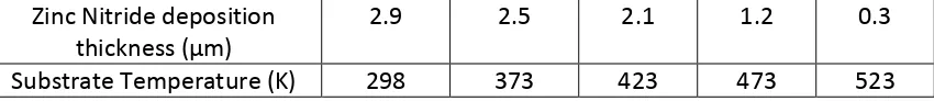
Temperature evaluation had been assessed on Silicon and glass substrates using RF magnetron sputtering. The evaluated temperature in the range of 298 K to 523 K (25°C to 250°C) and results showed that the deposition thickness had inversed proportional effect towards the substrate performance which can be referred to Table 1.
Zinc Nitride deposition thickness (µm)
2.9 2.5 2.1 1.2 0.3
Substrate Temperature (K) 298 373 423 473 523
Table 1: Layer thickness performance versus substrate temperature
5
Figure 2: Electrical properties results towards the substrate temperature
The refractive index n had been calculated as well using the transmittance data based on the two lower valley observed in the graph shown in Figure 3. The refractive index were calculated based on below formula which in the range of 2.51 to 2.69 with the layer thickness d in the range of 1300 – 2300 nm.
n = [2 d(1/λ2 – 1/ λ1)] -1
6
Based on Zhang June [6] even though the objective of the project to generate Zinc Oxide on glass substrate, the method that being used was developing the Zinc Nitride first using the reactive magnetron sputtering approach. The Zinc Nitride being deposited first by using metallic Zinc disc with Gallium grain as the target which initially being sputter by Argon gas for 30 minutes to remove any target contamination at 40 sccm flow rate. The N2 – Ar were based on 50% mixture and sputtering time setting was
30 minutes with 120 W DC Power. The substrates temperature being set with two setting which room temperature and 200°C with setting towards high temperature Zinc Nitride claimed has smoother surface performance.
There was some analysis towards oxidation on the Zinc Nitride films towards the oxidation time. In 1 hour the result showed that the structure of Zinc Nitride has partially changing to Zinc Oxide with increasing of oxidation time at 500°C and at 2 hours the Zinc Nitride was completely changed to Zinc Oxide. This data could be referred to Figure 4 for reference. This is a very important information in order to avoid the oxidation occurred during the sputtering process.
Figure 4: X-ray diffraction results of Zn2N3 substrates at 500°C with different oxidation time [7]
7
room temperature up to 400°C. The base pressure was set low at 10-6 Torr range with 80W RF Power at 5 minutes with Argon gas environment.
The usage of Zinc Nitride sputtering target had been assessed [9] by V.Kampylafka which was the backup plan that had been identified in this project if the Zinc target is not working. Results showed n-type Zinc Nitride deposited in pure Argon gas using RF Magnetron sputtering. The optical band gap of Zinc Nitride been reported having a range between 1 to 3eV depending the deposition method .The Zinc Nitride target was initially pre sputtered using Argon plasma with 5mTorr pressure, 100W RF power within 15-20 minutes deposition time. The Zinc Nitride then being deposited at 100W RF power, 5mTorr total pressure setting with mixture of Argon and Oxygen gases. The distance between target and substrate was 11 cm. Annealing was done at 400°C convert most of the Zinc into Zinc Nitride but small amount of oxygen residuals detected in the annealing process. Conductivity reported in the range of 10-2 to 101 Ω cm which depending on the deposition thickness. Zinc Nitride improved the conductivity after annealing at 300°C however annealing at higher temperature claimed to have higher resistivity and transparent physical appearance.
Another method being used for getting wider band gap (1.01 eV to 3.02 eV) Zinc Nitride from V.Kambilafka [10] which using the RF magnetron sputtering with Argon and Nitrogen gas mixture. The wide band gap material being produced to make it a suitable candidate for optoelectronics transparent devices. The Zinc Nitride deposition was based on 100W RF power with 5 mTorr pressure on unheated glass substrates. The deposited materials then went through thermal treatment with temperature up to 550°C. The results reported that with gas mixture of 20% Nitrogen and 80% Argon, substrates thermal treatment at 150 °C provided higher conductivity and mobility during the investigation while using 100% Nitrogen plasma the films were too resistive to be measured by the Hall effect measurements.
There was an approach using Ammonia (NH3) gas which being mixed with Argon
gas to generate the Zinc Nitride deposition method using RF magnetron sputtering. The deposition was done on unheated glass substrate with the Zinc target distance 60mm from the substrate. The mixture of NH3 and Ar gas being varied with the total flow rate 20 sccm. The NH3 flow rate setting were 1-5 sccm and balance mixture with Argon will
8
Figure 5: Effects of NH3 ratio towards Zn3N2 (321) on X-ray diffraction
From the listed literature reviews, all the parameters that being used towards the sputtering activities had been compiled for referencing purpose. It is important to understand the key parameters that being used for the Zinc Nitride deposition process. The evaluation should be carried out to understand the capability of DC magnetron sputtering in The University of Sheffield and verify the effects of each defined parameters.
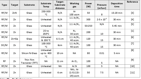
2.1 List of previous parameter compilations
9
Type Target Substrate Substrate
Temp
10
2.2 DC magnetron sputtering operating process
In general, DC magnetron sputtering was using high voltage application which consists of anode and cathode for operating process. The sputtering target (which in this evaluation using Zinc) connected to the cathode which represented as the negative output of the DC power supply while the substrate (glass substrate) will be connected to anode in a vacuum chamber. The selected gas atoms then will be hitting the target and the target material will deposit a thin layer onto the glass substrate which being connected to anode. The magnetron function ensures the gas atom which was previously in random movement attracted and then being directed to the sputter target. The magnet actually being allocated behind the sputtering target to create the magnetic field around the target. With low gas pressure and high voltage which flows from the magnetron, it generated high energy plasma to bombard the target resulting to target coating layer to deposit on the glass substrate. The magnetron process functioning could be clearly seen below in Figure 6 for reference.
Figure 6: Magnetron process functioning
11
12
Chapter 3: Overall evaluation methods and activities
3.0 Methodology
The evaluation methodology had been reviewed and discussed with supervisor prior starting the data collection. The Gantt chart for the overall activities being finalized and can be referred to Appendix 1 for details. The key objective of this project was to develop Zinc Nitride sputtering process using the existing DC magnetron sputtering equipment and study its electronic properties stability behavior based on Hall Effect measurement. Once the Zinc Nitride successfully developed, then the deposition layer will be analyzed to understand the performance versus time. Since the deposition results will need for Hall Effect measurement the glass substrates were cut into 8 x 8 mm from the original 22 x 22 mm size. The 8 x 8 mm being selected because to fit the Hall effect measurement board contact pin fitting which according to the 8 x 8 mm size. While for original glass substrate 22 mm x 22 mm will be used on Ellipsometer and Dektak surface profiler for Zinc Nitride thickness measurement activities. The glass substrate being manual cut using diamond pen to shape it.
13
Argon violet emitting colour Nitrogen pink emitting colour
Figure 7: Comparison of Argon and Nitrogen emitting colour
The sputtering operating process for DC Magnetron equipment can be referred to Figure 8 below. Zinc target which being connected to cathode being bombarded and the deposited Zinc will falls on the glass substrate that connected to anode in Nitrogen environment.
Figure 8: Illustration of process setup on DC Magnetron Sputtering equipment
The parameters that being assessed towards the deposition of the Zinc Nitride towards the glass substrate and had been identified and below are the list for reference
1. Gas Flow rate (sccm)
14 3. Substrate temperature (°C)
4. Nitrogen gas (fixed)
The Nitrogen flow rate being evaluated first to understand its performance towards Zinc Nitride deposition behavior. The parameter setting had been defined below in Table 3 for reference.
Table 3: Nitrogen flow rate assessment towards Zinc Nitride deposition performance.
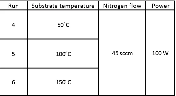
The substrate temperature then being assessed by referring to Table 4 for reference. The Nitrogen flow rate and power being fix for this parameter setting. These evaluations were continuation analysis from run 1, 2 and 3 performance which involve various Nitrogen flow rate assessment.
Table 4: Substrate temperature assessment towards Zinc Nitride deposition performance.
Run Nitrogen gas flow Temperature Power
20°C 100 W
Run Substrate temperature Nitrogen flow Power
4 50°C
45 sccm 100 W
5 100°C
15
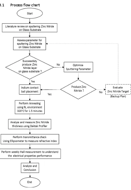
The overall process flow can be referred in Figure 9 for reference.
3.1 Process flow chart
16
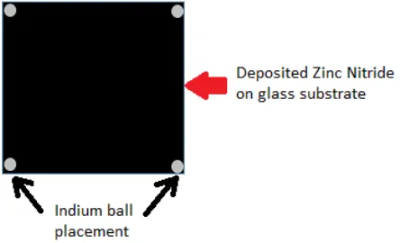
3.2 Indium ball placement
Indium ball placement being prepared for Hall Effect measurement activities. It being setup for jig contact point which indicated in Figure 10 below for Van der Pauw technique.
Figure 10: Four probe jig for Van der Pauw technique
Below are the steps on how the Indium ball placement being done. Big chunk of Indium had been cut manually using tweezer and then roll the Indium with glass substrate until it become thin and long. This method being done to simplify the process by cutting into small pieces. The rolled Indium samples will be soaked in n-Butyl Acetate which being placed on the hot plate with temperature of 400°C. Then the rolled Indium sample being soaked in Acetone and Isopropyl Alcohol in order to clean it and avoid from any contaminations. It will be dried using air gun and being cut into small pieces using tweezers. Then allocate the small pieces of Indium at 4 corner of the deposited glass substrate as illustrated on Figure 11.
17
Once the Indium balls placement completed then the annealing process took place. Annealing was performed in Nitrogen environment with temperature 320°C for 1.5 minutes. All samples then went for Hall Effect measurement using four pin probe Van der Pauw technique.
3.3 Hall Effect definition
Edwin Hall had discovered in 1879 when an electrical current being applied through a metal/semiconductor samples, a difference of voltage difference known as Hall voltage will be produced with the presence of magnetic field. The voltage transverse to the electric current while the magnetic the magnetic field perpendicular to the current. Hall Effect measurement is a method to extract important electrical properties such as sheet resistance, sheet carrier density, doping type (n or p type material) and mobility.
3.4 Hall Effect measurement configuration setup
The electrical properties for the Zinc Nitride checking were based on the Hall Effect measurement. The Hall Effect systems consists of 5 components which can be referred in Figure 12 below.
18
Component 1 (Ecopia HMS5000 dual magnet assembly)
- contains a permanent magnet with different polarity setting. The evaluation samples with the board will be allocated in this area and there is a liquid nitrogen reservoir which can be used in this component as well.
Component 2 (Connection cable)
- functioning as electrical connection from the evaluation sample towards the connector box for measurement purpose
Component 3 (Connector box)
- consist of 4 bananas socket which being labelled as A, B, C and D. Functioning as a connector for current and voltage source. The positioning will be changed according to the contact point for current supply and voltage measurement.
Component 4 (Keithly 6220 precision current source)
- deliver a constant DC with current source ranging of 0.1 pA to 0.1 A which connected to the samples by the red and blue connectors.
Component 5 (Keithly 2700E multimeter)
- being connected with yellow and green banana connectors and used for voltage measurement from the samples.
19
Figure 13: PCB sample board (left) and connector box (right)
The connector box linked by banana clips which differentiate by its colour which can be referred in Figure 14.
For voltage source Yellow banana clip (represents positive terminal) and
Green banana clip (represents negative terminal)
For current source Red banana clip (represents positive terminal) and
Blue banana clip (represents negative terminal)
![Figure 4: X-ray diffraction results of Zn2N3 substrates at 500°C with different oxidation time [7]](https://thumb-ap.123doks.com/thumbv2/123dok/491940.54407/11.612.132.523.304.575/figure-ray-diffraction-results-substrates-different-oxidation-time.webp)