Digital Frequency
Synthesis
Demystified
DDS and Fractional-N PLLs
Bar-Giora Goldberg
a volume in the Demystified seriesEagle Rock, VA
Goldberg, Bar-Giora.
Digital frequency synthesis demystified / Bar-Giora Goldberg. p. cm.
“A volume in the Demystified series.” Includes bibliographical reference and index. ISBN 1-878707-47-7 (pbk. : alk. paper)
1. Frequency synthesizers--Design and construction. 2. Phase -locked loops. 3. Digital electronics. I. Title.
TK7872.F73G55 1999
621.3815 486--dc21 99-34856
CIP
Copyright © 1999 by LLH Technology Publishing.
All rights reserved. No part of the book may be reproduced, in any form or means whatsoever, without written permission from the publisher. While every precaution has been taken in the preparation of this book, the publisher and author assume no responsibility for errors or omissions. Neither is any lia-bility assumed for damages resulting from the use of the information contained herein.
Printed in the United States of America 10 9 8 7 6 5 4 3 2 1
Cover design: Sergio Villareal Developmental Editing: Carol Lewis Production: Kelly Johnson
Eagle Rock, VA
Prefaces xi Symbols xv
Chapter 1. Introduction to Frequency Synthesis 1
1-1 Introduction and Definitions 1
1-2 Synthesizer Parameters 5
1-2-1 Frequency Range 6
1-2-2 Frequency Resolution 6
1-2-3 Output Level 7
1-2-4 Control and Interface 7
1-2-5 Output Flatness 7
1-2-6 Output Impedance 7
1-2-7 Switching Speed 7
1-2-8 Phase Transient 8
1-2-9 Harmonics 9
1-2-10 Spurious Output 10
1-2-11 Phase Noise 10
1-2-12 Standard Reference 13
1-3 Auxiliary Specifications 13
1-4 Review of Synthesis Techniques 13
1-4-1 Phase-Locked Loop 14
1-4-2 Direct Analog Synthesis 21
1-4-3 Direct Digital Synthesis 26
1-5 Comparative Analysis 35
1-6 Conclusion 37
References 38
Chapter 2. Frequency Synthesizer System Analysis 39
2-1 Multiplying and Dividing 39
2-2 Phase Noise 42
2-3 Spurious and Phase Noise in PLL 49
2-4 Phase Noise Mechanism 51
2-4-1 Noise in Dividers 51
2-4-2 Noise in Oscillators 51
2-4-3 Noise in Phase Detectors 52
2-5 Mixing and Filtering 53
2-6 Frequency Planning 55
References 56
Chapter 3. Measurement Techniques 57
3-1 Switching Speed 57
3-2 Phase Noise 61
3-2-1 FM Noise 62
3-2-2 Delay Line Discriminator 63
3-2-3 Integrated Phase Noise 66
3-2-4 Noise Density 66
3-3 Phase Continuity 66
3-4 Spurious Signals (Especially DDS) 67
3-5 Phase Memory 69
3-6 Step Size 69
3-7 Linear FM 70
3-8 Conclusion 70
References 71
Chapter 4. DDS General Architecture 73
4-1 Digital Modulators and Signal Reconstruction 75
4-2 Pulse Output DDS of the First Order 82
4-3 Pulse Output DDS of the Second Order 87
4-4 Standard DDS 89
4-4-1 Binary-Coded Decimal DDS 100
4-5 Randomization 105
4-5-1 Wheatley Procedure 106
4-5-2 Randomizing Sine Output 108
4-6 Quantization Errors 109
4-6-1 Digitized Model 109
4-7 Logic Speed Considerations 120
4-8 Modulation 120
4-9 State-of-the-Art Components and Systems 128 4-9-1 Very High-Speed Direct Digital Synthesizer 128 4-9-2 Medium-Speed Direct Digital Synthesizer 129
4-10 Performance Evaluation 133
4-10-1 Switching Speed 133
4-10-2 Phase Noise 133
4-10-3 Spurious Signals 134
4-10-4 Phase Continuity 134
4-10-5 Resolution 134
4-11 Sample-and-Hold Devices 134
4-12 Single-Bit DDS Revisited 135
4-13 Arbitrary Waveform Generators 138
4-14 Digital Chirp DDS 140
4-15 Conclusion 140
Appendix 4A DDS Applications 141
Appendix 4B DDS—Spectra and the Time Domain 143
Appendix 4C Sampling Theorem 157
Appendix 4D The Effect of Phase Noise on Data Conversion Devices 159
Chapter 5. Phase-Locked Loop Synthesizers 163
5-1 Main Components of PLL Synthesis 164
5-1-1 Voltage Controlled Oscillators 165
5-1-2 Analog Phase Detector 168
5-1-3 Digital Phase Detector 1 172
5-1-4 Digital Phase Detector 2 175
5-1-5 Digital Phase Detector 3 176
5-1-6 Digital/Analog Phase Detector 4 177
5-1-7 Dividers 180
5-2 Performance Evaluation 184
5-2-1 Wireless PLL ASIC Configuration 198
5-3 Fractional-NSynthesizers 201
5-3-1 Fractional-NSynthesis of the First Order 204 5-3-2 Fractional-NSynthesis of the Second Order 216 5-4 Fractional-NSynthesis of the Third Order 220
5-5 DDS-Based PLL 224
5-5-1 Speed Up 226
5-6 Single-Chip PLL Synthesis 227
5-7 Conclusion 230
References 235
Chapter 6. Accumulators 237
6-1 Binary Accumulators 237
6-2 Decimal Accumulators 245
6-3 Interface to ROM 246
6-4 Accumulator DDS 248
6-5 Phase Adder and Accumulator Segmentation 248
6-6 Conclusion 250
References 250
Chapter 7. Lookup Table and Sine ROM Compression 251
7-1 ROM Algorithm 252
7-2 Quadrant Compression 256
7-3 Compression Principles 259
7-4 Direct Taylor Approximation 260
7-5 Hutchison Algorithm 262
7-6 Sunderland Algorithm 266
7-7 Variations and Randomization 269
7-8 Auxiliary Function ROM Approximation 271
7-8-1 Spurious Signal Analysis 274
7-9 Coordinate Transformation (CORDIC) 275
7-10 Other Methods 278
7-11 Conclusion 279
Chapter 8. Digital-to-Analog Converters 281
8-1 DAC Performance Evaluation 282
8-2 DAC Principles of Operation 285
8-3 DAC Parameters 292
8-3-1 Update Rate 292
8-3-2 Resolution 292
8-3-3 Logic Format 293
8-3-4 Setup-and-Hold Time 293
8-3-5 Rise, Fall, and Settling Times 293
8-3-6 Propagation Delay Time 294
8-3-7 Differential Linearity 294
8-3-8 Integral Nonlinearity 294
8-3-9 Monotonicity 295
8-3-10 Multiplying Bandwidth 295
8-3-11 Glitch Energy 295
8-3-12 Symmetry 296
8-4 State-of-the-Art DACs 296
8-4-1 Low-Speed Operation 296
8-4-2 Medium-Speed Operation 298
8-4-3 Very High-Speed Operation 298
8-4-4 Other Recommended DACs 299
8-5 Sine-Wave DAC 299
8-6 Multiplexing 299
References 303
Chapter 9. Synthesizers in Use and Reference Generators 305
9-1 Synthesizers in Use 305
9-1-1 Hewlett-Packard 3325B 306
9-1-2 Hewlett-Packard 8662A 307
9-1-3 Program Test Sources 310 307
9-1-4 Comstron/Aeroflex FS-2000 309
9-1-5 Schomandl Models ND500 and ND1000 309
9-1-6 Stanford Research DS345 309
9-2 Reference Generators 313
9-2-1 General Review 314
9-2-2 Crystal Oscillators 316
9-3 Conclusion 319
References 319
Chapter 10. Original Paper and Software 321
10-1 Tierney, Rader, and Gold Article 321
10-2 Software Description 322
This book—the latest volume in our popular Demystified series of technical references—is an updated version of an earlier text, Digital Te chniques in Frequency Synthesis, published by McGraw -Hill. In addition to the updated text, a CDROM has been added that contains an assortment of design tools, including an informa-tive new reference in pdf format from Analog Devices calledA Te chnical Tutorial on Digital Signal Synthesis. The CDROM also i n cludes a fully searchable pdf file of the entire book contents. Fo r a full list of the CDROM contents, see Chapter 10.
ABOUT THE AUTHOR
Bar-Giora Goldberg received his education at the Technion-Israel Institute of Technology in Haifa, and he worked there for 10 years in communication and spread-spectrum systems. In 1984 he cofounded Sciteq Electronics, a world leader in the field of digital frequency synthesis, and he now heads Vitacomm, a company dedicated to frequency and time engineering products for wireless and high-speed telecommunications. Giora has writ-ten exwrit-tensively, has been awarded several pawrit-tents, and has been a major contributor to the introduction and development of DDS and fractional-N technologies. He is also associated with Besser Associates in the US and Continuous Education International (CEI) in Europe, companies dedicated to continuous education via seminars and on-line courses.
As in the first edition of this book, my purpose is to present to the designer a comprehensive review of digital techniques in modern frequency synthesis design. The text specifically addresses prac-tical designers, and an attempt has been made to approach the subject heuristically, by using intuitive explanations and includ-ing many design examples.
Not long ago, frequency synthesis was considered a novelty. It was used in the more complex and demanding applications. Today, frequency synthesis is so ubiquitous that it is not even possible to say that its use is growing. Frequency synthesis is now so natural that every radio design uses only synthesized sig-nals for generation and control. This is partly because the spectrum is so precious a commodity, and its use is controlled tightly by government and industry. Other reasons include the increase in complexity of modulation, the phenomenal increase in use, and the increase in convenience. No more dialing and fine-tuning; just push the button, and the channel is locked in with an accuracy that does not require correction.
Frequency synthesis therefore has entered the age where it is used in applications such as military radios, satellite communi-cations terminals, and radars as well as in CB radios and hi-fi consumer electronics. It is not possible to consider the huge acceleration of cellular telephony and the still emerging markets of wireless and personal communications services (PCS) without the use of frequency synthesis.
Frequency synthesis is a fascinating technological discipline, as it includes both analog and digital technologies. To design a synthesizer one has to apply a great variety of disciplines such as oscillators, voltage-controlled oscillators, amplifiers, filters, phase detectors, logic, and low-noise dc amplification and filter-ing. This book, however, is not intended to be a general introduction to frequency synthesis; rather, it tries to focus on a segment of the technology.
There has obviously been a trend to “go digital” in the last 15 to 20 years. Although they are usually more complicated than ana-l o g, digitaana-l technoana-logies offer exceana-lana-lent repeatabiana-lity, much better a c c u r a c y, improved performance, and repeatability in production. This trend has not been ignored by frequency generation tech-n o l o g i e s. There have beetech-n major advatech-nces itech-n two key t e ch n o l o g i e s. The first is known as direct digital synthesis (DDS), a technology that generates the signal digitally and converts it via a digital-to-analog converter (DAC) to a sine wav e. This tech-nology is almost purely within what is known today as digital signal processing (DSP), but it has been in development for over 15 years within the domain of radio-frequency (RF) electronics e n g i n e e r i n g. The second is the digitalization of phase-locked loop (PLL) tech n o l o g y, the one that is the most popular and probably covers 98 percent of frequency synthesis and its evolution to what is referred to today as f r a c t i o n a l-Ns y n t h e s i s.
Even very recent texts on PLL frequency synthesis have defined the technique as “generation of frequencies which are exact multiples of a reference.” This definition is not accurate anymore. The more advanced synthesizers generate frequencies that are related to the reference but are not always exact multi-ples. In fact, the very principle of fractional-N PLL synthesis requires that the ratio of output frequency to the reference be a rational fraction. It so happens that these PLL technologies are also closely related to DDS and as such include DSP, a discipline that will find increased applicability in signal generation in the years to come.
This text was written mainly as a consequence of the rapid developments of these technologies and the lack of literature, especially the two subjects mentioned above. To the best of my knowledge, no other text exists that attempts to focus on the modernization and digitalization of signal generation.
Frequency synthesis, and especially the digital part of it, is now going through a major evolutionary period. Modern systems require high levels of integration, low power dissipation, and low cost. Digital technologies fit this bill precisely and allow the push in the technology. Frequency synthesis has received much atten-tion from chip manufacturers, and a great variety of PLL and direct digital synthesizer chips have been available for several years. We are now seeing a major shift from the standard PLL to fractional-NPLL and a major increase in the use of DDS. These technologies are used in cellular and PCS applications as well as disk drives and satellite communications terminals. What can be more exciting and faster-moving than these markets today?
The collection of files on the accompanying CDROM has been provided to help the reader analyze and manipulate methods described in the text. The software has been devised for IBM PC compatibles, but it will also be applicable for Macs.
I would like to take this opportunity to thank former and cur-rent colleagues who contributed to this book while working with me or discussing various aspects of the technical details. No one can do it alone. A text like this presents a set of ideas and tech-niques that evolved through the ages, and personally through many years of practice. It is therefore not possible to mention all the people who made a contribution to the maturization of the technology of accurate timekeeping, but I am indebted to them.
I would like to extend my thanks to my friends and family, especially Pnina, who encouraged and supported this very long, hard effort. I would like to specifically thank my Technion men-tors, Dr. Jacob Ziv and Israel Bar-David; and Henry Eisenson, a great friend, a brother, and a partner who always helps by giving support and encouragement.
a angle
AM amplitude modulation
b angle
c angle
CORDIC coordinate transformation DAC digital-to-analog converter
dB decibel
dBC dB referred to carrier
dBm dB over 1 mW
DDFS direct digital frequency synthesizer DDS direct digital synthesis
Er, er error
fi input frequency
fm modulating frequency
Fo output frequency
Fr, Fref reference frequency
FM frequency modulation
Fs sampling frequency
gcd(a, b) greatest common divisor
H(x) transfer function int(x) integer of x
IF intermediate frequency
Kd phase detector gain constant
K0 VCO gain constant
Lm(fm) SSB noise density at fmfrom the carrier, in dBC/Hz
LFM linear FM
LSB least significant bit
m index of modulation
MSB most significant bit
NCO numerical control oscillator PM, fM phase modulation
RF radio frequency
S sum (usually at accumulator output)
SSB single sideband
T sample time
VCO voltage-controlled oscillator
a angle
b angle
j damping factor
f phase
v radial frequency
vn natural frequency
1
1
Introduction to
Frequency Synthesis
1 - 1 I n t roduction and Definitions
This text deals with emerging modern digital techniques used to generate and modulate sine wav e s. These waveforms are used in almost all radio applications, communications, radar, digital com-m u n i c a t i o n s, electronic icom-maging, and com-more. Such tech n i q u e s either build the waveform from the “ground up” digitally (i.e., gen-erate all the signal parameters such as phase, frequency, and amplitude digitally) and deal with the very fundamental nature of the waveform and its features (direct digital synthesis) or are part of the digital heart of modern p h a s e - l o cked loop(P L L) synthesiz-e r s. This might ssynthesiz-esynthesiz-em, and is indsynthesiz-esynthesiz-ed, a common and known subjsynthesiz-ect. Sine waves are truly natural waveforms and trigonometric func-tions that are well known and have been researched for a long t i m e. Furthermore, frequency synthesis is quite a mature tech-nology with extensive literature and comprehensive coverage in the professional meetings. Why another text on the subject? What is new besides application-specific integrated circuit(A S I C) tech-nologies and silicon densities, geometry, and integration?
elec-tronics and other very popular applications at extremely low cost (and the popularization of frequency synthesis from consumer products all the way to complex requirements) is the advance of digital technology; integrated, high densities; and low-cost silicon single-PLL chips and ASICs. However, parallel to the advance of traditional PLL synthesis, there emerged other synthesis tech-n i q u e s, maitech-nly digital itech-n tech-nature, direct digital synthesis(D D S) and fractional-N PLL synthesis. Thus, the classical PLL synthe-sizer is now being supplemented with a sizable element of digital t e chnology and digital signal processing(D S P). Indeed the appli-cation of DSP techniques to frequency synthesis is still at an early s t a g e.
The generation of sine waves by using digital methodologies requires generating the waveform from the ground up. This is fun-damentally different from the PLL synthesizer, where the signal is available from an oscillator. It goes back to the very basic struture of the waveform itself and deals with its very basic ch a r a c-teristics rather than manipulates signals that have already been generated by an oscillator. Surprisingly, some of these very basic mathematical issues are being resolved only lately.
U n f o r t u n a t e l y, in these specific fields, there is a lack of complete understanding of the mathematics as well as the standard imple-mentation of working hardwa r e. The operation of a direct digital synthesizer is far from intuitive, and its artifacts are sometimes alien to our (conservative or standard) thinking. Indeed, in this ongoing research effort, we have tried to recruit some very skilled professional mathematicians in the search for (1) effective sine r e a d - o n ly memory(R O M) (the transformation of wto sinw) com-pression algorithms (indeed, the same old trigonometric func-tions; see Chap. 7), (2) a “minimal” amount of data necessary to represent the waveform, such as to meet a specific level of accu-r a c y, and (3) a geneaccu-ral foaccu-rmulation foaccu-r the peaccu-rfoaccu-rmance of DDS. We have not had much luck or enthusiasm.
We understand that this might not be the most exciting topic for m a t h e m a t i c i a n s, but it has tremendous importance for electron-i c s, radelectron-io, and radar deselectron-igners. The challenge has to be met welectron-ithelectron-in the electronics community, and we have attempted to present a comprehensive introduction.
first attempt to write a comprehensive text on the subject of digi-tal frequency synthesis, direct digidigi-tal synthesis, and digidigi-tal and f r a c t i o n a l -N synthesis; and the number of sources is not over-whelming in this newly emerging technological discipline. We h ave found a paucity of literature in the field; and even though many articles have begun to appear in the last few years and the t e chnology attracts much attention in professional meetings, com-prehensive texts and bibliographies are needed. This is what this text attempts to supply. Every attempt is made to present a very c o m p r e h e n s i v e, updated bibliography.
Because of the paucity of literature, in this text we attempt to present an intuitive approach supplemented by many examples, in the hope that this book fills a current need as expressed to us by many young and beginning designers as well as others who are not familiar with the details and lack an intuitive under-standing.
In this text, a frequency synthesizeris defined as a system that generates one or many frequencies derived from a single time base (frequency reference), in such a way that the ratio of the output to the reference frequency is a rational fraction. The fre-quency synthesizer output frefre-quency preserves the long-term frequency stability (the accuracy) of the reference and operates as a device whose function is to generate frequencies that are multiples of the reference frequency (multiples by a single or many numbers). These multiples may be whole or fractions; but since only linear operations are used (in the frequency domain), these numbers can only be rational. A frequency synthesizer, as defined here, can thus generate an output frequency of, say,X/Y (where X and Y are whole numbers) times the reference fre-quency, but not, for example,ptimes the reference frequency (p is not a rational number).
Another synthesizer technique is known as direct analog(D A) frequency synthesis. In this tech n i q u e, a group of reference fre-quencies is derived from the main reference; and these frefre-quencies are mixed and filtered, added, subtracted, or divided according to the required output. However, there are no feedback mech a n i s m s in the basic tech n i q u e.
The DA frequency synthesis technique offers excellent spectral p u r i t y, especially close to the carrier, and excellent switching speed, w h i ch is a critical parameter in many designs and determines how fast the synthesizer can hop from one frequency to another.
The DA technique is usually much more complicated than PLL to execute and is therefore more expensive. DA synthesizers found applications in medical imaging and spectrometers, fast-switch-ing antijam communications and radar, electronic warfare(E W) simulation, automatic test equipment (ATE), radar cross-section ( R C S )measurement, and such uses where the advantages of the DA technique are a must at a premium cost.
The third tech n i q u e, which is the focus of this book, is direct digital synthesis (DDS), which is a digital signal processing (DSP) discipline and uses digital circuitry and techniques to cre-a t e, mcre-anipulcre-ate, cre-and modulcre-ate cre-a signcre-al, digitcre-ally, cre-and eventucre-ally convert the digital signal to its analog form by using a d i g i t a l t o -analog converter(D AC).
Although the direct digital synthesizer [sometimes referred to as n u m e r i c a l ly controlled oscillator(N C O)] was invented almost 30 years ago (see Ref. 9 and Chap. 10), it started to attract attention only in the last 10 to 12 years. Due to the enormous evolution of digital technology and its tools, the technique evolved remarkably into an economical, high-performance tool and is now a major fre-quency synthesis method used by almost all synthesizer designers from instrument makers to applications like satellite communica-t i o n s, radar, medical imaging, and cellular communica-telephony and amacommunica-teur radios (most of which are anything but amateur).
Another focal point of this text is the description of fractional-N PLL synthesis. This technique resembles DDS in almost all aspects and operates as a DDS “inside” the PLL arch i t e c t u r e. Please note that in many designs, more than one synthesis tech-nique is being utilized, and the designer “hybridizes” the design so that the advantage is taken of each technique being used and its weaknesses are suppressed. So it is quite common (and applica-tions can be expected to grow) to see combinaapplica-tions of PLL and DDS or DA and DDS, and from time to time all three tech n i q u e s are used in one design. Thus the basic three techniques indeed complement one another and enable the up-to-date competent designer to use all as needed to optimize the design as the appli-cations and demands increase with the system complexity.
This text has 10 ch a p t e r s. Chapter 1 is a general introduction and short description of frequency synthesis tech n i q u e s, Chap. 2 deals with synthesizer system analysis, and Chap. 3 addresses measurement techniques pertinent to frequency synthesis. Chap-ter 4 details a variety of DDS technologies and deals with the quantization effects, their artifacts, and representations in DDS. Chapter 5 discusses PLL principles and the details of fractional-N PLL synthesis of various complexities. Chapters 6, 7, and 8 deal in detail with the cardinal components of DDS, namely, accumu-lators of binary and binary-coded decimal (B C D) structure, ROM lookup tables and ROM compression algorithms, and digital-to-analog converters. Chapter 9 gives a short review of state-of-the-art reference oscillators and what we consider some remarkable instruments or products on the market that are directly related to digital frequency generation.
Chapter 10 is special, as it refers to a reprint of the original 1971 a r t i cle by Tierney, Rader, and Gold that kicked off the DDS indus-try (Ref. 8), including some footnotes. This article is special not only because of its pioneering nature but also for the fact that it deals with all the cardinal issues of the subject. The chapter also i n cludes a description of the programs contained on the accompa-nying CDROM.
1 - 2 S y n t h e s i zer Pa r a m e t e rs
most common specifications is provided followed by a definition and industry standard conventions. Obviously, for different appli-c a t i o n s, different speappli-cifiappli-cations are more important than others, and it is up to the designer to design for efficiency and economy. While a FS for a car radio needs to be moderately accurate, extremely reliable, very small and simple, and very inexpensive, a FS used in magnetic resonance imaging(M R I) must be very accu-r a t e, must have veaccu-ry high spectaccu-ral puaccu-rity, must be able to hop faccu-rom frequency to frequency very quick l y, and needs different modula-tion capabilities. While consumer electronic products need to oper-ate in extreme environmental conditions (one expects the car radio to operate when powered up in extreme heat or cold condi-t i o n s, and condi-the vibracondi-tions of condi-the cars are severe), condi-the MRI spec-trometer operates in a laboratory-controlled environment with lit-tle temperature variation and almost no shock or mech a n i c a l v i b r a t i o n s.
Designers are therefore required to compare their specifications to the best economical and practical solution. The specifications are divided into two groups: those that are related to the topics of this book and others that are more general and are beyond our s c o p e. All the following sections pertain to generic specifications.
1 - 2 - 1 Frequency range
This specifies the output frequency range, including the lower and higher frequencies that can be obtained from the FS. The units of frequency are hertz (Hz), or cycles per second.
1 - 2 - 2 Frequency resolution
1 - 2 - 3 Output level
The output power level is usually expressed in decibels (0 dBm is 1 mW). The output power can either be fixed, say,110 dBm, or can cover a range, say,2120 to115 dBm. This specification will also i n clude the output power resolution, for example, 1 dB or 0.1 dB.
1 - 2 - 4 Control and interface
This parameter specifies the control methodology and the inter-face to the FS. The control can be binary-coded decimal (BCD) or binary; it can be parallel or via a bus (usually an 8-bit bus) or ser-ial; it can be transparent or latched. When the control is latch e d , there is a register that receives the control word and upon activa-tion (by a latch command) loads the control word into the FS (also referred to as double buffering). Some FSs use positive logic and others use negative; and in many general-purpose instruments, GPIB or IEEE-488 is currently the standard interface. VXI is an emerging new interface standard for instrumentation.
Most single-chip synthesizers, especially PLL, make extensive use of the serial interface to allow small packages and highly inte-grated functionality.
1 - 2 - 5 Output flatness
This parameter specifies the flatness of the output power and is measured in decibels (dB). For example, the output power is spec-ified as 10 dBm 61 dB, where dBm means decibels over 1 milli-watt (mW).
1 - 2 - 6 Output impedance
This parameter specifies the nominal output impedance of the FS and usually is also the recommended load impedance. In most radio-frequency and microwave equipment, this is 50 ohms (V). In video it is usually 75 Vand in audio equipment 600 V.
1 - 2 - 7 Switching speed
para-m e t e r. In sopara-me applications the requirepara-ment is to settle to within a specific frequency (6xHz) from the desired new frequency (say, 50 Hz or 5 kHz from the desired frequency). Suppose that the specification is to cover 10 to 100 MHz and switch to within 1 kHz in less than 100 microseconds (ms). To measure this parameter, a counter is set to measure the new frequency (say the FS is com-manded to hop between 10 and 100 MHz periodically) and is timed to start measuring only 100 ms after the command bit is activated (say, for 5 ms, because the time allowed must be short relative to the specification time). If the measurement is either 10 or 100 MHz (depending on where we command the counter to measure) within 6 1 kHz, then the specification has been met. Obviously in such a measurement a pulsed counter must be used, and its gating time must be specified, too.
A more common and more demanding specification defines the s w i t ching speed by the time it takes the output phase to settle to 0.1 rad of the final phase.
If the FS generates Acos (v1t1 w1) and is controlled to a new frequency, say,Acos (v2t1 w2), the signal phase will go through a transient from v1t1 w1to v2t1 w2and eventually will settle at v2t1 w2. The standard definition of switching speedis the time it takes the switching transient to achieve an output phase of v2t1 w260.1 rad (approximately 5.7°). Note that in most cases w1and w2are not a part of the measurement since their values are not a parameter in the overall system and the user does not care about their values. But from time to time stringent require-ments arise where the phase is also specified relative to some given reference. See Chap. 2.
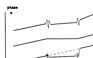
1 - 2 - 8 Phase transient
In most applications, the behavior of the phase when in a tran-sient state is not defined, as shown in part aof Fi g. 1-1. However, many applications need to define the transient ch a r a c t e r i s t i c s very carefully. Two typical requirements are as follows:
Figure 1-1 Phase switching in transition.
is important when one is attempting to generate a synthesized s w e e p, also known as linear FM, and has many applications in m e a s u r e m e n t s, EW, radar, and specific modulations [e. g., m i n i -mum shift keying(M S K)]. Such a phase transient is smooth and generates very little “noise,” and this is very desirable in systems and networks.
1-2-8-2 Phase memory switching. This means that if the FS runs at f1and then is switched to f2,f3,f4, … and back to f1, then it will resume the phase where it would have been if it were run-ning continuously at f1, as shown in part cof Fig. 1-1.
This requirement is simple to achieve if all the output frequen-cies are generated simultaneously and are switched to the specific output (f1, f2, f3, …) upon command. In such a case, every genera-tor will continue to oscillate even when it is not used, and there-f o r e, when it is reconnected, it will preserve its phase. However, ithere-f a single switched output is used, this requirement is sometimes quite tricky to achieve (see Ref. 12). Many applications require s u ch a feature, e. g., coherent pulse Doppler radar imagers that frequency-hop but use coherent pulse detection (for predetection i n t e g r a t i o n ) .
1 - 2 - 9 H a r m o n i c s
1 - 2 - 1 0 Spurious output
This specification defines the level of any discrete output fre-quency spectral line not related to the carrier. Most users do not consider harmonics as spurious signals. However, subharmonics, because of either multiplications or those that appear as DDS arti-f a c t s, are considered spurious signals even though they are some-times specified separately. This parameter is expressed in decibels relative to the carrier output power. Unlike noise, spurious signals are only discrete spectral lines not related to the carrier, meaning that they exhibit periodicity.
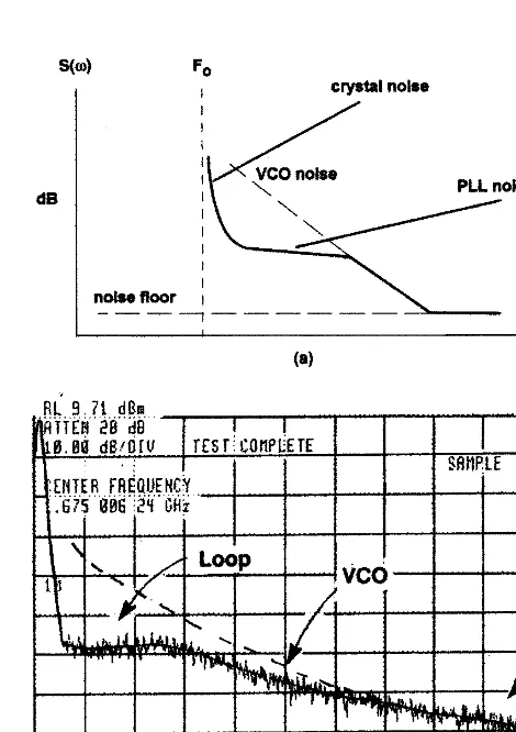
1 - 2 - 1 1 Phase noise
From the purist’s standpoint, there are no deterministic signals in the real world! All real signals are narrow-band noise. Every sig-nal we generate is derived from an oscillator. Oscillators are posi-tive feedback amplifiers with a resonance circuit in their feedback path. Since noise always exists in the circuit, upon power up this noise is amplified in the resonator band until a level of saturation is achieved. Then the oscillator passes from the transient to its steady state. Thus, the quality of the signal is mainly determined by the resonator Q. The signal that we usually refer to as a “sine wave” is actually narrow-band noise. The quality of the signal is determined by how much of its energy is contained close to the car-r i e car-r. The centecar-r fcar-requency is actually the avecar-rage—the mean—of the noise frequency. Phase noise in a way is the standard devia-tion of the noise. In very high-quality signals, like crystal oscilla-tors (Qrange of 20,000–200,000), 99.99% of the signal energy can be contained within .1 Hz of the center frequency.
This parameter specifies the phase noise of the output carrier relative to an “ideal” output. The ideal output of a sine-wave gen-erator is given by
Asin (v0t1 w) (1-1)
and its presentation in the frequency domain is a delta (Dirac) function at angular frequency v0:
F(v)5A⋅ δ(v 2 v0) (1-2)
has an ideal bandwidth of zero. Such a signal must be of infinite time (otherwise its spectrum will have a finite width greater than zero) and infinite power. However, the reference to a delta function is convenient for theoretical evaluations. High-quality frequency synthesizers generate signals which contain 99.99 percent of their energy in less than 1 Hz of bandwidth around the carrier. Crystal oscillators can contain 99.99 percent of their energy in less than 0.01-Hz bandwidth.
O b v i o u s l y, in the real world the only signals we can generate are given by
A[11n1(t)]sin[v0t1n2(t)1 w] (1-3)
where n1(t) represents the amplitude instability and n2(t) repre-sents the phase perturbations, both relative to the ideal case. These noise functions are random by nature and represent a spec-trum that has to be designed to meet a specification.
Figure 1-3 Integrated phase noise. S/N5signal/noise in 30 kHz (excluding 2 Hz around the carrier).
quite complicated, and the instruments necessary to make the measurement are quite expensive.
Another method of defining phase noise is to measure the inte-grated noise in a given bandwidth around the carrier but excl u d-ing 61 Hz around the carrier. This is shown in Fi g. 1-3. Obviously this method is related to the first one by the integration of the noise energy under the phase noise curve. However, compared to phase noise measurement, this is a simple measurement to m a k e. The information available from such a measurement is a good indicator of the overall performance of the unit; but since this is an integrating measurement, the total noise power is mea-sured even though its detailed spectral shape is lost. Tradition-ally (probably because of applications related to voice), the noise bandwidth is measured between 1 Hz and 15 kHz. So the mea-surement is the ratio of the total signal power to its noise from 1 to 15 kHz from the carrier (30 kHz of noise bandwidth). As an i n d i c a t o r, high-quality VHF/UHF synthesizers achieve a ratio of 60 to 70 dB and better.
fluctuations it is possible to infer the spectrum of the signal. All these methods are related mathematically and must be consistent with one another. For detailed analysis of phase noise, see Chap. 2 and Refs. 13 and 14. Usually the FS phase noise reaches a noise f l o o r, as shown in Fi g. 1-2, and this parameter is sometimes spec-ified, too. [A program to convert L(fm) to root-mean-square degrees is included on a disk the reader may obtain from the author (see C h a p. 10).]
1 - 2 - 1 2 Standard reference
Since all synthesizers use a reference time base input, this speci-fies the reference frequency (usually 5 or 10 MHz, but there are many others), and its parameters such as stability, phase noise, spurious signals, and power level.
1 - 3 Au x i l i a ry Specifications
These specifications are usually related to the execution of the specific synthesizer but are not dealt with here. Usually they i n clude parameters such as size, power supply requirements, environmental factors, quality, and reliability.
1 - 4 R ev i ew of Synthesis Te ch n i q u e s
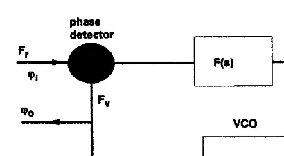
Figure 1-4 PLL block diagram.
Figure 1-5 VCO control characteristics and piece-wise linearization.
1 - 4 - 1 Phase-locked loop
As mentioned before, the phase-locked loop (PLL) is by far the most popular frequency synthesis tech n i q u e. It is basically a non-linear (the phase detector is a nonnon-linear device) feedback loop, as shown in Fi g. 1-4. The PLL consists of a voltage controlled oscilla-tor (VCO), a phase detecoscilla-tor, a variety of dividers, and a loop filter. The VCO is a device whose output frequency depends on the input control voltage. The relation is nonlinear (a typical response is shown in Fi g. 1-5) but monotonic. However, when locked, the VCO can be assumed to be linear; it is both practical and conve-nient for analytical purposes. Variation in the VCO control ch a r-acteristics (i.e., this nonlinearity) affects the loop parameters, and loop linearization (or compensation) is used extensively. Gener-a l l y, the VCO output wGener-aveform is given by
where Ais the signal amplitude and v is the angular frequency, both depending on time t ,and control voltage v.
As a first approximation, we assume that Ahas a constant enve-lope (does not depend on tor v) and that vis a linear function of v. Therefore we can write Eq. (1-4) as
Aout(t)5Asin[(v01Kvv)t1 w] (1-5)
Here Kvis the VCO constant [rad/(V⋅s)]. Since we assume that the frequency is linearly dependent on vand is given by
v(v)5 v01Kvv (1-6)
as mentioned, the linearization is justified and is assumed for the purpose of simpler analysis. In reality, when the loop is locked, fre-quency variations are tiny, and the constant-VCO assumption is correct as a piecewise linearization of the graph in Fi g. 1-5.
Since phase is the integral of the angular frequency, we can complete the approximation by writing that the VCO transfer function, given by
5 (1-7)
as the Laplace transfer function of the VCO output phase.
The phase detector produces an output voltage proportional to the difference in phase between its inputs and is always a nonlin-ear function. Typical phase detector output transfer functions are shown in Fi g. 1-6. However, close to the locked position this
func-Kv
s wo(s)
V
tion can be assumed to be linear (this is also justified since in the l o cked condition most frequency synthesizers operate with a very high signal-to-noise ratio and the phase detector therefore oper-ates mainly at a fixed-phase position). Hence
Vd5Kd(wi2 wo) V/rad (1-8)
where Vdis the phase detector output voltage.
Now the loop transfer functions can be described as
Vd5Kd[wi(s)2 wo(s)] (1-9)
L e t
Vc(s)5Vd(s)F(s) control voltage (1-10)
where F(s) is the loop filter transfer function and Vc is the VCO control voltage. Solving these simple equations yields
wo(s)5 (1-11)
and the transfer function H(s)5 wo(s) /wi(s) is given by
H(s)5 (1-12)
A l s o, following these equations will show that the error transfer f u n c t i o n ,defined as
He(s)5 (1-13)
is given by
He(s)5 (1-14)
Since we linearized all components, given Kvand Kd,the feedback loop behavior depends mainly on F(s) .
Also note that the error function has high-pass ch a r a c t e r i s t i c s, and therefore a true direct-current (dc) modulation of a PLL cir-cuit is not possible. This function, however, also referred to as d c frequency modulation,is possible in other synthesis tech n i q u e s.
s
s1KdKvF(s) wi(s)2 wo(s)
wi(s) KdKvF(s)
s1KdKvF(s) wi(s)KdKvF(s)
1 - 4 - 1 - 1 First-order loop. A first-order loop is obtained when F(s) 5 constant, say, A . This means that the loop filter has a fixed gain but no dependence on frequency. The gain is neces-sary because of the difference between the output voltage of the phase detector and the required control voltage input to the V C O. (Most phase detectors produce output voltage levels of 0 to 2 or 5 V while the VCO control might require 10, 15, and some-times 24 or even 50 V to cover its operating range. )
In this case, the loop transfer function wo(s)/wi(s) 5 H(s) reduces to
H(s)5 (1-15)
For convenience we shall designate
K5KvKdA (1-16)
and rewrite H(s) for a first-order loop:
H(s)5 (1-17)
As can be seen, this loop leaves few options to the designer since the loop parameters Kv, Kd,and Adictate the behavior of the feed-b a ck mechanism. Note that there is only one integrator in this PLL (phase is the integral of frequency, and the VCO ch a r a c t e r i s-tics in the Laplace domain have been described as Kv/s) and there-fore only one pole in the transfer function. An intuitive approach to the loop behavior can be taken by realizing that the transfer function is that of a single-pole low-pass (R C) filter. So, for a step in the input phase, say wi,the output phase will be given by
wo(t)5 wi(12e2t/K) (1-18)
and the phase error will be given by
wo2 wi5 wie2t/K (1-19)
This assumes that the input phase step is fixed. This shows imme-diately that in such a loop, fixing Kv, Kd,and Adetermines imme-diately the dynamics of the loop and its noise b a n d w i d t h (B W) , w h i ch is defined by
K
s1K KvKdA
BW5
E
∞
0 |H(jv)|
2df (1-20)
and is given by K/ 4 .
The noise BW of a PLL is an indicator of the loop bandwidth, and its calculation presents the integrated bandwidth of the loop and a measure of its speed of response.
The transfer function of a first-order loop is similar to that of an R Cfilter; and the error transfer function e(s), indicating the error after a transient has settled, e(s) 5He(s)wi(s), is given by
e(s)5 5 (1-21)
The error function can be calculated for a phase step by using the final-value theorem, which states that steady state in the time domain can be calculated from the transfer function in the fre-quency domain. Accordingly, for a phase step wi,the final value of the error is given by
5lim
s50 sX(s) (1-22)
where X(s) is the Laplace transform of x(t) and is therefore in this case
lim s = 0
50 (1-23)
Thus a phase shift in the input will be tracked by the output. How-e v How-e r, a phasHow-e ramp, or a frHow-equHow-ency How-error dv, yiHow-elds
lim
s = 0 5 (1-24)
Thus a first-order loop when one is tracking a phase ramp (fre-quency change) will generate a fixed phase error, proportional to dvand K.Obviously higher-level changes in the phase rate (par-abolic and higher) cannot be tracked and create a diverging error. With only one integrator (the VCO) in the loop, this is expected.
This PLL structure is not particularly popular for FSs because of its lack of degrees of freedom in the design.
dv
K dv
s1K swi }
s1K −∞x t
( )
+∞
∫
s
s1K e(s)
wi(s) swi(s)
1 - 4 - 1 - 2 Second-order loop. This model of the PLL is the most commonly used in the FS industry. Although many designers claim that in reality there are no second-order loops (since the devices used to realize the loop filter always add poles), this rep-resents an approximation to an analysis that is simple and yields a good theoretical approximation of the behavior of the majority of PLL designs. In this case
F(s)5 (1-25)
[note the added integrator in the network F(s)] and
H(s)5 (1-26)
Following the common notions of control theory, we define
(1-27)
a n d
j 5 (1-28)
and the transfer function can now be represented as
H(s)5 (1-29)
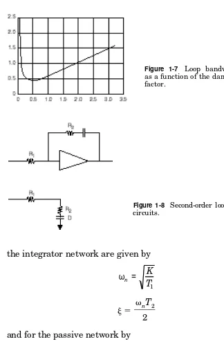
As in most second-order control systems, the characteristics are controlled by vn,also called the loop natural frequency, and the damping factor j (both designators imported from control the-ory). Such a loop can be controlled by F(s) to arbitrary jand vn, and it can be shown (Ref. 1) that the loop BW, as defined in Eq. (1-20), is given by
BL5 (1-30)
as shown in Fi g. 1-7 .
The loop filter is usually realized by either a passive network or an active integrator, as shown in Fi g. 1-8. The design equations for
vn }}
2(j 11/4j) 2jvns1 vn2
}} s212sv
nj 1 vn2 vnT2
} 2
ωn = K T1
K(sT2 +1) /(T1)
s2+s(1+KT2) /(T1)+K/(T1)
11sT2
Figure 1-8 Second-order loop c i r c u i t s .
the integrator network are given by
(1-31)
j 5 (1-32)
and for the passive network by
(1-33)
j 5 (1-34)
vn(T211/K) }}
2
ωn = K T1 +T2 vnT2 }
2
ωn = K T1
Figure 1-9 PLL for frequency synthesis.
Note that Kdis in volts per radian, Kvin rad/(s?V), Kin 1/s, and vnin radians per second; jis dimensionless.
In PLL synthesizers, the output of the VCO is usually followed by a divider, as shown in Fi g. 1-9. In the lock conditions, the out-put frequency will be given by N Fr e f, and so by changing N, t h e output frequency is changed. All the equations stay the same, except the VCO constant changes from Kvto Kv/ N .
The transfer function is given by
H(s)5 (1-35)
For a second-order loop, it can be shown that the steady-state error for a step input and for a linear phase ramp dvis 0 (there are two integrators in the loop), but a parabolic phase rate (linear FM) cannot be tracked and a frequency error is generated. Obviously h i g h e r-order loops are used for applications where higher- l e v e l phase changes are required, but the majority of PLL applications, especially for frequency synthesis, use second-order designs.
1 - 4 - 2 Direct analog synthesis
Unlike PLL, the direct analog (DA) technique uses arithmetic operations in the frequency domain (but no closed-loop feedback mechanisms) to convert the input reference signal to the required output frequency. The main tools for the DA technique are therefore comb generators, multipliers, mix and filtering, and division.
KF(s)
Figure 1-1 0 Direct analog design using multiple references. BPF 5bandpass filter.
Because such operations are complex, it is desirable to design repeating building block s, so that their production will be eco-nomical; otherwise, price and complexity are both very high.
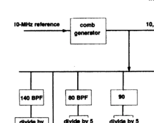
To demonstrate the basic elements of the DA tech n i q u e, we con-sider a tentative design of a synthesizer that covers 16.0 to 16.99 MHz of output frequency range, has 0.01-MHz (10-kHz) step size, all derived from a 10-MHz reference. This demonstration design ( Fi g. 1-10) requires the following reference frequencies: 14, 16, 18, 20, 22, 130, and 131 MHz. Given these reference frequencies, the generation of which is not necessarily trivial, a common block might look like that in Fi g. 1-10.
Note that the output of the first stage serves as the input to the second stage (similar), and so at the output of the first stage 10 fre-quencies will be generated, from 16.0 to 16.9 MHz, but at the out-put of the second, the complete range of 16.0 to 16.99 MHz is a chieved (100 frequencies). Note that by adding more similar s t a g e s, the resolution of the synthesizer can be increased to any required level. The same stage can therefore be used repeatedly without the need to generate more references.
Figure 1-1 1 Reference generation for DA design.
method is demonstrated in Fi g. 1-11. The 10-MHz comb generates 10-MHz comb lines 10, 20, 30, …, 140 MHz. The 14 is generated by 140/10 (or 70/5), the 16 by 80/5, the 18 by 90/5, the 20 by 120/6, the 22 by 110/5, the 130 by 120 110 (both available), and the 131 by 120 (available) 1110 (av a i l a b l e ) / 1 0 .
This architecture usually operates in blocks of decades and is used here to demonstrate the DA principles. There can be many other variations, but this is quite a typical and efficient design. The basic element of DA is therefore mix and filter.
Note that the spectral purity depends on the spectral purity of the references (usually excellent), and the speed of the synthesizer in this case depends on the speed of the switches that switch in and out the reference frequencies and the response time of the filters.
The above design can achieve switching speeds of 3 to 10 microseconds (ms) depending on the detailed design.
Note also that if all the above operations were designed at fre-quencies 5 times higher, the filter’s bandwidth would hav e increased 5 times and the speed would depend mainly on the speed of the switch e s. Such a design could achieve submicrosecond speed. Obviously the compromise will involve cost.
all the references run continuously, they all maintain phase mem-o r y. The prmem-oblem mem-occurs in the divider. We knmem-ow that mix and filter preserve the phase of the references since it is basically a s i n -g l e - s i d e b a n d(S S B) operation that can be expressed as
ej(v1t1 w1)?ej(v2t 1 w2)5ej[(v11 v2)t 1 w11 w2)] (1-36)
and the phases are preserved. However, the divider (here by 10) will suffer a transient, and its output phase can be at any one of 10 possible output phase states, and so the phase preserva-tion is lost. Therefore, there is no phase continuous switch i n g in such a design, and this means that linear FM sweeps cannot be generated.
As a general rule for such block decade design, the output fre-quency is given by
Fout5Fi1 1 1…5Fi1
^
nj51
Fj(102j) (1-37)
where Fiand Fjare the inputs to the block .
In the above case, if N50 were the last stage and did not con-tain the divide-by-10 device common to all other stages, then the output frequency range would be 160.0 to 169.99…and the num-ber of 9s (or the resolution) depends on the numnum-ber of stages being employed. This is convenient for two reasons: the frequency coverage is 10 MHz (rather than 1 MHz for the common block ) , and the final frequency is higher and easier to convert upwa r d .
Early DA designs were quite complicated, had many crystal ref-erences in them, and had complex arch i t e c t u r e s. All this is gone n o w. All DA designs consist of repeatable block s, which imply effi-ciency in production and elegance.
Another technique that is usually associated with DA is called drift canceland is worth mentioning. The general idea is demon-strated in Fi g. 1-1 2 .
A comb generator is used to generate a comb spectra line, in this example 50 MHz apart, and a free-running VCO and a b a n d p a s s f i l t e r(B P F) are used to output only one line at a time.
In the example, the VCO will be tuned to 2000 MHz to output 500 MHz. If the VCO is tuned to 2050 MHz, the output will be 550 MHz; the VCO tuned to 2100 generates 400 MHz; and so on. Note that the mathematical operation here is
Figure 1-1 2 Drift-cancel loop used in DA synthesizers.
Fout5FVCO2(FVCO2Fcomb line)5Fcomb line (1-38)
The VCO serves an auxiliary function and cancels itself. The VCO can be free-running since the level of accuracy necessary is only to bring the desired comb line into the BPF passband.
Although this is a simple, elegant, and economical tech n i q u e, the design is usually more complicated than it shows. Excellent isola-tion must be maintained to eliminate leakage of undesired comb l i n e s. In addition, the cancellation effect must be calculated rela-tive to the phase noise of the free-running VCO. Ideally the two VCO paths should have the same delay, and the signals should cancel perfectly. In reality, this is not the case, and the cancellation effect is finite. It is usually very good close to the carrier, but degrades as we move away from the carrier. The reason is cl e a r because the cancellation takes the form w(t)2 w(t1T), where Ti s the difference in the delay path of the two branches w 5 v0t1n(t) . Thus the cancellation takes the form
wn5 v0T1n(t)2n(t1T) (1-39)
d B. This causes most DA designs that use this technique (and this is attractive because of simplicity and cost) to have a relatively (to PLL) high noise floor, in the order of 2130 to 2135 dBC/Hz, in ultrahigh frequency(U H F). (Here dBC indicates decibels referred to c a r r i e r.) At a premium, the VCO can be replaced by a synthe-s i z e r. DA synthe-synthesynthe-sizersynthe-s will not be disynthe-scusynthe-ssynthe-sed in thisynthe-s text in great d e t a i l .
1 - 4 - 3 Direct digital synthesis
DDS is an emerging and maturing signal generation tech n o l o g y. Up to 10 years ago, this technique was rather a novelty and wa s used in very limited applications. However, due to the enormous evolution of digital technologies (speed, integration, power, cost), digital signal processing (DSP), and data conversion devices, it is becoming increasingly popular, and its performance improves c o n s t a n t l y.
There is a fundamental difference between DDS and DA or PLL. Although both PLL and DA techniques use digital devices, s u ch as dividers and phase detectors, the PLL and DA tech n i q u e s are fundamentally analog disciplines. The basic signal generator in both techniques is an oscillator, which is a feedback - t u n e d amplifier set to operate under specific conditions (controlled insta-bility). The oscillator is manipulated to allow the generation of a range of frequencies. In DDS, the signal is generated and manip-ulated digitally from the “ground up,” and after all the digital manipulations are completed, it is converted to an analog signal via a digital-to-analog converter (DAC ) .
The DDS is thus a computing machine where signals are repre-TABLE 1-1 Typical Noise Cancellation of 2.5-MHz
Drift-Cancel Loop
(Delay between cancellation paths is approximately 1 µs )
Offset from carrier (Hz) Cancellation (dB)
13103 45
13104 30
53104 20
13105 15
53105 5
sented by numbers and should be considered a DSP discipline. There are many compelling reasons to do this.
Signal generation is, after all, the heart of every electronic device and top of the list of standard industrial reasons to “go dig-i t a l .” Other engdig-ineerdig-ing drdig-ivers such as producdig-ibdig-ildig-ity, repeatabdig-il- repeatabil-i t y, relrepeatabil-iabrepeatabil-ilrepeatabil-ity, and very hrepeatabil-igh accuracy demand the use of drepeatabil-igrepeatabil-ital t e ch n i q u e s, which now infiltrate not only DSP but also signal gen-eration. DDS adds dimensions not possible with analog designs. In a way there is some similarity between the evolution of DDS and that of digital recording and the use of the compact disk(C D) . The signal has high fidelity, waveforms have been converted to numbers (an old Pythagorean dream come true), there is total con-trol of the signal parameters at all times, and the density of digi-tal circuitry allows a very high level of integration in small size e c o n o m i c a l l y.
T h u s, after years of maturity, DDS is finding many applications and has been established as a fundamental and important signal generation discipline.
1-4-3-1 Basic theory. Like most DSP disciplines, the funda-mental root of DDS is based on the sampling theorem, due to Shannon (see Chap. 4). The theorem states that any (stochastic, with finite energy) signal having a band-limited spectrum (i.e., the signal has no energy at frequencies above v0 5 W), such a signal can be represented by its discrete samples in time, pro-vided that the sampling rate is at least 2F0, where F05 v0/2p. A simple proof is provided in Chap. 4.
The sampling theorem shows that such a signal can be fully recovered from its samples and that, in the process, many other frequencies are being generated. These “artifacts” are also referred to as the aliasing signals. (See App. 4A.) We will demon-strate an intuitive explanation of what is happening in the sam-pled data domain.
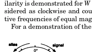
Suppose that a viewer sits in a dark room. In front of her there are a wheel and a single bar connecting the center of the wheel to the perimeter. Suppose also that a light source is set behind her and flashes very short flashes (almost like a delta function sam-pling) at the rate of 10 flashes per second.
describe what is happening in front of her eyes, she will not be able to give a conclusive answer. Note that what the viewer sees (which is the reality in this case) is the bar advancing 36° cl o ckwise at every flash. Her interpretation will be that the wheel is rotating at 1 Hz, or 11 Hz, or 21 Hz, or at any frequency that is 1 0n11 Hz cl o ck w i s e, but also at 9 Hz or 19 Hz or any frequency that is 10n21 Hz countercl o ck w i s e.
This is a cardinal point in DDS theory. The same results will be observed by the viewer if the bar is rotated at 10n11 or 10n21 , or generally n (light sampling) 6 K (wheel frequency) rotations per second.
This interpretation of the experiment is, of course, the spectrum shown in the mathematical proof of the sampling theorem. The mathematical proof is enlightening by itself. We can interpret the cl o ckwise rotations as positive frequencies and the countercl o ck-wise rotations as negative frequencies. These negative frequen-cies are obviously as real as the positive ones and in DSP termi-nology are usually referred to as the aliasing frequencies.
A special interesting case arises when the rotation is exactly 5 Hz. At this point, all the positive and negative frequencies con-v e r g e. This is referred to as the Nyquist frequency(half the sam-pling rate).
In DDS, the procedure of the signal sampling is reversed. And the process is therefore reversed. Suppose that, instead of sam-pling a sine wav e, we generated its samples. (All can be calculated since the waveform is known; the sine is a perfectly known wav
form, unlike a stochastic process that is random by nature.) Then according to the theorem it will be possible to reconstruct the sine wave signal perfectly.
In essence, that is what DDS is. The rest is details and tech-niques for efficient, economical, and fast executions.
1-4-3-2 DDS concepts. There are a great variety of DDS imple-mentations, as will be demonstrated in Chap. 4. However, the dominant one consists of four elements: an accumulator, a sine lookup table, a DAC, and a low-pass filter (LPF). See Fig. 1-14. Remembering that the presentation of a amplitude, fixed-frequency, and fixed-phase sine wave is given by
Asin(vt1 w) (1-40)
we can trace the signal buildup as follows: The signal phase is a linear function, as shown in Fi g. 1-14. The gradient or slope of the phase dw/d tis the angular frequency v. To generate the amplitude of the output waveform, it is necessary to transform the phase w(t) to sin[w(t)], and this is usually done by using a read-only memory (ROM), since the transformation is nonlinear and ROM (or RAM) is a convenient tool.
The accumulator is a device that performs the function
S(n)5S(n21)1W (1-41)
S u ch a device is a digital integrator and produces a linear output ramp whose slope (rate of change) is given by W,the input control word. This device is used to generate the phase vtor in the sam-ple data W?n?T,where Tis the sampling time and depends on the
cl o ck at which the accumulator runs. The accumulator is operat-ing as an indexer whose output (representoperat-ing the phase) controls the input to the ROM (or lookup) sine table, and can be viewed as a complex, yet easy to engineer and control, counter.
Suppose that the accumulator size is N bits, say N 5 32 bit binary device. It is therefore able to accumulate from 0 to 23 221 .
Obviously, above this number the accumulator will overflow and start again from 0. The rate of accumulation depends only on the clock rate Fck51/Tand W.And Wcan be as low as 0—in this case the accumulator will not increment (equivalent to generating a dc signal)—or any arbitrary number W < 2N 2 1, which is the case if all the N inputs equal 1. If we equate 0 with zero phase and 23221 with 2p, then we have a device that generates phase
from 0 to 2pperiodically (since the device operates modulo 232),
as shown in Fig. 1-14. Figure 1-14 shows a typical cycle wave-form, and Fig. 1-15 shows that incrementing 1 or 23121 actually
causes the same (but reverse phase, see Chap. 4) effect.
We have already seen that in sample data systems the aliasing is the “shadow” (or image or reflection) of the signal, and their sim-ilarity is demonstrated for W51 or W523 221. They can be
con-sidered as cl o ckwise and countercl o ckwise or positive and nega-tive frequencies of equal magnitude.
For a demonstration of the operation of the accumulator, let us
Figure 1-1 5 Signal and aliasing. S(n+1) = S(n) + (1/12)
assume that we cl o ck the device, an N 5 32 bit accumulator, at Fck523 2/10. Then if W51, it will take exactly 10 s (2Ncl o ck tick s ) to generate 0 to 2p. However, if W 5 23 0, then it will take only
4 0 / 23 251 0 / 23 0s (four cl o ck ticks). Obviously Wcontrols the rate
of change of the accumulator, and the rate of change of the phase is the frequency v. In the above example, for W 51, the cycle is 1/10 or 0.1 Hz, while for W523 0the cycle is equal to 23 0/10 Hz, or
Fck/4 Hz.
M a t h e m a t i c a l l y, since v 5dw/d t ,we can rewrite
Fout52p 5 5 (1-42)
where Fo u tis the output frequency and Tis the cl o ck time. For this e x a m p l e, the cycle frequency will be given by
Fout5
o r
Fout5 (1-43)
where ACM is the maximum number of states of the accumulator. Equation (1-43) is a generic equation for DDS.
Note that for all practical purposes, W < 2N21, because that is
the Nyquist frequency and the point of conversion between the frequency and its “shadow” or aliasing.
Not all accumulators are binary, and we will mention others later (see Chap. 4).
The phase information is connected to the ROM which converts vtto sinvtor wto sin w. Since the accumulator is usually large and the memory size is limited, only part of the accumulator output bits is connected to the ROM. For example, if the 14 most sig -nificant bits(M S B s) of the accumulator are connected to the ROM and we require 12-bit output from the ROM to drive a 12-bit DAC, then the size of the required memory is 21 4312, which is
equiva-lent to approximately 192,000 bits of memory and is already quite a large ROM. More on the ROM and ways to compress its size will be discussed later (Chap. 7).
We have introduced a level of truncation since not all the accu-FckW
} ACM FckW } 232
FckW } 2N W
2N/T dw
mulator bits are connected to the ROM. The error will be evalu-ated in Chap. 4.
The digital output bits of the ROM, which converted the phase information to amplitude, are now connected to the DAC and low-pass filter that generate the analog sine wave. The LPF rejects all aliasing frequencies and is therefore theoretically lim-ited to the Nyquist frequency. It is sometimes referred to as the antialiasing filter.
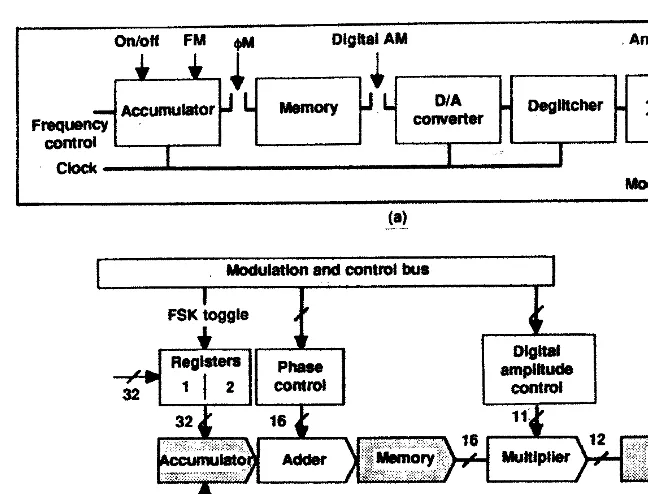
1-4-3-3 Modulation. Since we have total control of the signal parameters, it is easy to include modulation ports to add fre-quency, phase, and amplitude modulation, all in the digital domain, as shown in Fig. 1-16.
Frequency is changed by changing the value of W,w h i ch is the basic function of the direct digital synthesizer. Because of the nature of DDS, phase continuous switching is simple to ach i e v e. Note also that dc FM is possible in DDS. Sometimes when dc FM is required from a PLL system, it is done by locking the PLL to a direct digital synthesizer, and it is FM-modulated. The phase is changed by inserting an adder between the accumulator and the ROM, and this function is shown in Fi g. 1-17. Adding (or subtracting) a number causes a phase shift. And amplitude is changed by inserting a multiplier between the ROM and the D A C.
If all modulations are employed, the output waveform will be given not as
Asin (vt1 w) (1-44)
but rather as
A(a) sin [v(W)t1 w(b)] (1-45)
Thus total digital control of the signal parameters has been a chieved; see Fi g. 1-16. Such devices that employ all digital mod-ulations [and more, such as built-in linear FM (chirp) functions and standard functions like ramp and sinx/x] are available in the market now.
Gambar
Dokumen terkait
[1] Having both encrypted and non-encrypted password clients on your network is another reason why Samba allows you to include (or not include) various options in the
But the Category link on the Web search results page is helpful in a surprising way: When you want to see pages similar to the target page, Google Directory is better than the
If a digital camera had unlimited memory capacity, and file transfers from the camera to your computer were instantaneous, all images would probably be stored in RAW or TIFF
No matter what sample size you have, there is a value that is different from the hypothesized mean by an amount that is so small that it is quite unlikely to get a
(Remember that with equal access, if you want to make calls on a secondary carrier, i.e., not your primary carrier, all you would need do is dial 10XXX (XXX being the
Finally, take the latitude and longitude returned from Eventful and store it in your cache—you can use the information in the local cache the next time you need to look it up..
If you don’t want Windows to hide icons in the notification area, right-click a blank area of the taskbar and choose Properties from the context menu. On the Taskbar tab of the
The ODP-CAC scheme is able to achieve this for newly originating calls, by allocating bandwidth to the lower priority class which got a lesser resource either from the unused bandwidth
